Abstract
In this paper we study the uniformity of up to150 mm in diameter wafer-scale Ill-V epitaxial transferto the Si-on-insulator substrate through the O2 plasma-enhanced low-temperature (300°C) direct wafer bondingVoid-free bonding is demonstrated by the scanning acousticmicroscopy with sub-um resolution. The photoluminescence (PL) map shows less than 1 nm change in averagepeak wavelength, and even improved peak intensity (4%better) and full width at half maximum (41% better) after150 mm in diameter epitaxial transfer. Small and uniformlydistributed residual strain in all sizes of bonding, whichis measured by high-resolution X-ray diffraction Omega2Theta mapping, and employment of a two-period InPInGaAsP superlattice at the bonding interface contributes tothe improvement of PL response. Preservation of multiplequantum-well integrity is also verified by high-resolutiontransmission electron microscopy.
1 Introduction
Progressive developments in the semiconductor industrysince the invention of integrated circuits has resulted inhigh-quality mirror polished, fiat large area semiconduc-tor wafers which meet the requirements for good large-scale wafer bonding [1, 2]. Wafer-scale bonding is an attractive approach in hybrid integration for low-cost, large-throughput electronic and optoelectronic production. Thehybrid silicon platform developed recently [3, 4] relies onthe high-quality InP-based multiple quantum-well (MOW)active region transfer to the silicon-on-insulator (SOl) substrate through a low-temperature direct wafer bonding [5.6]. Bonding uniformity over the entire bonded area is ofgreat importance to ensure device yield and performanceuniformity, particularly for dissimilar material bonding withdifferent coefficient of thermal expansion. In this paper westudy the direct bonding uniformity of 50, 100 and 150 mmin diameter InP-based as-grown epitaxial layers transferredonto the SOI substrate. Parameters of interest, including thedistribution of interfacial void, strain, photoluminescence(PL) response, and bonding interface, are characterized bythe high-resolution scanning acoustic microscopy (SAM).X-ray diffraction (XRD) wafer mapping, PL wafer mappingand transmission electron microscopy (TEM), respectively.
2 Experiment
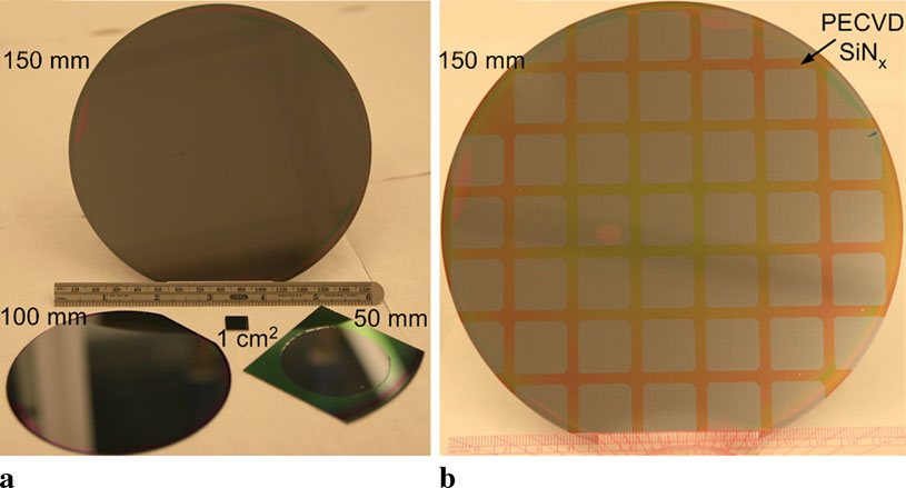
Standard 100 and 150 mm in diameter (001) SOI waferswere used for mating with InP-based epitaxial wafers in 50100 and 150 mm diameters. Waveguide circuits and vertical outgassing channels [6] were patterned on the silicon-on-insulator (SOl) wafers prior to bonding process. The150 mm in diameter Ill-V wafer contained a metallorganicchemical vapor deposition (MOCVD)-grown, diode laserstructure with 8-period, compressively strained (1%), un-doped InGaAsP quantum wells (Ag = 1.54 um) and dopedInP layers. Ill-V wafers in smaller sizes are composed ofthe MOCVD-grown, undoped 2 um InP and 100 nm In-GaAs etch stop layers. Thorough wafer cleaning and the02 plasma surface activation are conducted, followed bymating at room temperature and anneal at 300°C with 1-2 MPa external coaxial pressure. Then the InP substrateis selectively removed in a wet etch, leaving ~2 um thickIll-V epilayers on the SOl substrate with InGaAs etchstop layer on the surface. Detailed Ill-V epitaxial layerstructure and bonding process can be found in [6, 7]. Figure 1(a) shows the photo of thin Ill-V epilayers with different size (1 cm2,50, 100, 150 mm in diameter) on theSOl, demonstrating >98% area transfer and mirror-like IllV surface with a typical root mean square (RMS) surfaceroughness of 0.6 0.7 nm [7]. Further device process pro-ceeded on the 150 mm bonded sample. After putting alayer of 300 nm plasma-enhanced chemical vapor deposition (PECVD) SiN, at 260°C, standard projection photolithography and dry etch patterned the racetrack ring laserlayout with each device die (2 x 2 cm2). Wet etch then removed surface InGaAs layer in exposed area, giving us access to PL response from the active region. No extra delamination is observed during thermal cycling and wet processing, indicating strong, robust III–V-to-Si bonding.
3 Results and discussion
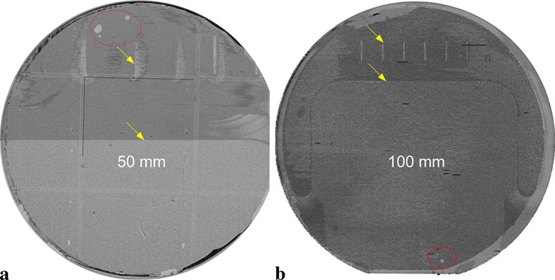
interfacial voids after removingTypically, we spot anythe thick InP substrate under the optical microscope inNormaski-mode whose resolution is good enough to resolvesub-um voids. Void-free bonding is achieved in randomlyselected area in all bonded wafers due to vertical outgassingchannels [7] to absorb the gas byproducts (H2O, H2) frominterfacial polymerization reactions and trapped N2, CO2.etc.[6]. Here we utilize the high-resolution SAM with sub-um resolution (X-axis: 0.5 um, Y-axis: 0.25 um, Z-axis:0.5 um) to show the entire wafer-scale images of 50 and100 mm bonded wafers in Fig. 2. Only are few relativelylarge voids (highlighted in red circles) were observed. Theyare close to the wafer edge and likely to be from surface par-ticles during manual wafer handling. No uniformly distributed, gas byproducts-resulted voids are found, which is com-patible with previous inspection in Normaski microscopy inselected areas [7]. Void-free bonding was observed in >99%of area. The misleading contrast and some vertical lineshighlighted in SAM images in Fig. 2 are from the waferchuck related to the SAM tool.

Figure 1

Figure 2
From a device point of view, preservation of designed active region after epitaxial transfer is most important to ourinterest. PL (Apump = 532 nm) maps measured at room tem-perature for the 150 mm InP MOW wafer prior to and after epitaxial transfer in Fig. 3 are compared to study thepotential material gain change from bonding and thermalprocess. Average PL peak wavelength of 1539.6 nm, average peak intensity of 5.444 V and average spectrum fullwidth at half maximum (FWHM) of 67.9 nm of the as-grown InGaAsP MOW epitaxial wafer are measured priorto the bonding. As mentioned before, the removal of the topInGaAs (Ag ~ 1.62 um) layer except the individual devicedie margin allows probing the true multiple quantum-well(MOW) luminescence data. The PL response from chip margin (i.e., PL response of the top InGaAs layer) is removedin the image and statistics for accurate comparison. AveragePL peak wavelength, peak intensity and FWHM after bonding and initial device processing are 1540.4 nm, 5.666 Vand 36.8 nm, respectively. Nearly no average PL wavelengthshift is measured (left column), indicating the small residual strain. Peak intensity (center column) and FWHM (rightcolumn) are even improved by respective 4% and 41% afterepitaxial transfer. Similar improvement has been reported inthe InP-to-GaAs bonded sample with placing several periods of the InP-lattice-matched InGaAsP/InP superlattice atthe bonding interface [8], which is also implemented in this work.
上一篇: 硅上磷化膜的光子集成
下一篇: 磷化铟光子集成电路技术