Abstract A summary of photonic integrated circuit (PICplatforms is provided with emphasis on indium phosphide (InP)Examples of InP PICs were fabricated and characterized for frecspace laser communications, Lidar, and microwave photonics. Anovel high-performance hybrid integration techniquetormerging InP devices with silicon photonics is also discussed.
I.INTRODUCTION
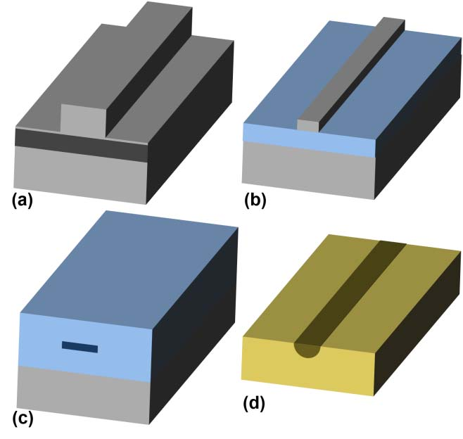
Photonic integrated circuit (PIC) technology continues tomature and expand in terms of functionality and performance1. Although silicon photonics (SiPh) has gained traction andpromises low-cost and high-volume production, indiumphosphide (InP) continues to be the most popular and advancedPIC platform (2],[3]. Aso, currently all SiPh PICs utilizeeither InP or gallium arsenide (GaAs) lasers for optical sourcesand rely on external coupling or heterogeneous/hybricintegration.Silicon nitride (SiN) has also received significant attentionas a low-loss passive waveguide PIC platform (4], (57. Lastlylithium niobate (LN) continues to be used widely for high.speed modulators for telecommunications.Figure I summarizes the primary PIC platforms illustratingcommon waveguide geometries used for each. The structureillustrated in Fig. 1(a) is referred to as a ridge or rib waveguideA common waveguide core is indium gallium arsenidephosphide (InGaAsP) while the cladding material is InPDepending on layer composition, thickness, and feature sizethe waveguide core optical confinement is considered to bemoderatefor InP.Thisdirectlydeterminesthesize/compactness of passive components and is also animportant consideration for the efficiency of active devices.

Figure 1
InP allows for the integration of all active componentsincluding lasers, semiconductor optical amplifiers (SOAs)photodetectors, and modulators. Depending on the complexityof the active-passive integration approach, low passivewaveguide loss can also be demonstrated
SiPh is based on silicon on insulator (SOl) technology andis illustrated in Fig. 1(b). Modulators based on pn junctions andphotodetectors have become mainstay activegermaniumcomponents for SiPh. The most common silicon device layerthickness is 220 nm and the buried oxide (BOX) layer istypically 2-3 um. This platform is characteristic of very highindex contrast (the refractive indices of the silicon core andoxide cladding are approximately 3.5 and 1.5, respectively at awavelength of 1.55 um) and therefore passive component sizesare extremely small. Unfortunately, modulation mechanisms insilicon are weak, therefore modulators are large in size despitethe high index contrast. SiPh also lacks an inherent lasertechnology and therefore techniques have been developed tointegrate compound semiconductor materials such as InP toprovide gain.
SiN can be considered as an alternative to traditional glasswaveguide technology that is based on doped silica. This is apassive PIC platform that could rely on hybrid orheterogeneous approaches to closely integrate activecomponents. SiN is used as the core guiding material andsilicon dioxide as the cladding material. Thicker waveguidecores (200-400 nm) can realize relatively strong opticalconfinement and in turn sharp waveguide bends and compactcomponents [6]. Thinner SiN cores (40-100 nm) can realizemore loosing confined waveguide modes and extremely lowpassive loss.
上一篇: InP硅集成的均匀性研究
下一篇: 磷化铟微系统的制造挑战