Abstract
Purpose - The purpose of this paper is to present a selective wet-etching method of boron doped ow-pressure chemical vapour deposition (LPCVDpolysilicon film for the realization of piezoresistors over the buk micromachined diaphraam of (100) silicon with improved yield and uniformity.)
Design/methodology/approach - The method introduces discretization of the LPCVD polysilicon film using prior etching for the grid thus dividinteach chip on the entire wafer. The selective etching of polysilicon for realizing of piezoresistors is imited to each chip area with individual boundaries
Findings --The method provides auniform etching on the entire silicon water irespective of its size and leads to economize the fabrication process in abatch production environment with improved yield.Research limitations/implications - he method introduces one extra process step of photolithoqraphy and subsequent etching for discretizing thepolysilicon film.
Practical implications -- The method is useful to enhance yield while defning metal lines for contat purposes on fabricated electronic structures usintmicroelectronics.Stress developed in LPCVD polysilicon can be removed using proposed approach of discretization of polysilicon film.
Originality/value - The work is an outcome of regular fabrication work using conventional approaches n an R&D environment. The proposed methodreplaces the costly reactive ion etching techniques with stable reproducibility and ease in its implementation.
Methodology of wet-etching process
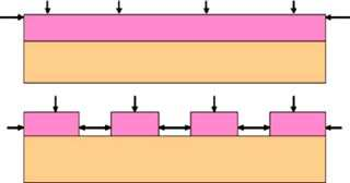
There are two situations ofwet etching ofpolysiliconthinlayer onthesilicon nitride/silicon dioxide cappedsiliconwaferas shown inFigure 1; blanket wet etching of polysilicon film with protectedpatterns of resistors over the entire surface, and second.discretization of polysilicon layer and then wet etching of eachunit simultaneously. In the previous situation etching rates ofpolysilicon is higher on the wafer edges and anon-uniform etchedpattern of remaining polysilicon is resulted. The size of arrowsshown in Figure 1 schematically shows the rate of etching whichis higher on the corners and slow on the flat surface.

Thediscretization ofthe polysilicon layer into smallsegments prior to the actual delineation ofpolysilicon resistors, enhances corners ina distributed manner on the entire polysilicon surface. The eachsmall independent island of polysilicon establishes its own etchrate according to its surface area and provides a better controlover the etching mechanism. By selection a uniform area of eachisland on the entire polysilicon surface, a uniform etchingrate canbe established. The geometry influence on the wet-etching ratehas been extensively studied in the literature (Koehler, 1999).Parameters related to reaction and diffusion mechanisms of wetchemical etching are strong functions of geometries to be etchedout. Fringing of reaction rates around sharp corners in thegeometry enhances the etching rates. With the decreasingdimensions ofthe structures to be defined by wet etching, moreinvolved etching mechanisms have been encountered in therecent studies (Yamamura and Mitani 2008).
上一篇: 多晶硅片表面过渡金属污染的影响
下一篇: 通过原子氢表面清洁实现GaAs晶圆键合