Abstract
Wafer level packaging (WLP) has been growing continuously in electronicspackaging due to its low cost in batch manufacturing and the potential of enabling wafertest and burn-in. A variety of wafer level packages have been devised, among which fourimportant categories are identified including thin film redistribution and bumpingencapsulated package, compliant interconnect, and wafer level underfill. This chapterreviews the different WLP technologies with an emphasis on challenges and processes ofthe wafer level underfill. The wafer level packaging integrated with wafer burn-in, testand module assembly shows great attraction due to the dramatic cost reduction. Costeffective ways of building wafer level test and burn-in are under investigation.
1. Introduction
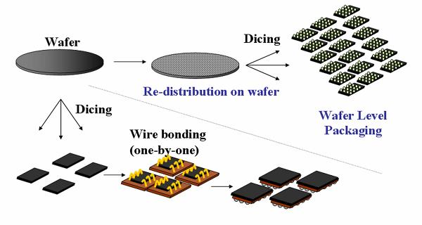
As a result of rapid advances in integrated circuit (IC) fabrication and the growingmarket for faster, lighter, smaller, yet less expensive electronic products, highperformance low cost packaging is needed by the electronics industry. The conventionaldiscrete IC packaging is inefficient, as such, a paradigm shift to wafer level packaging isapparent. Wafer level packaging (WLP) is a packaging technology where most or all ofthe IC packaging process steps are carried out at the wafer level. In the conventionaldiscrete IC packaging process, the wafers are diced into individual IC chips first and thenthe chips are redistributed and packaged individually. In the WLP process, redistributionand packaging are performed at the wafer level. After wafer dicing, the individuacomponents are ready to ship and assemble onto the substrates or printed wiring boards(PWBs) by the standard surface mount technology (SMT) process. A comparison of theconventional discrete packaging and the wafer level packaging is illustrated in Figure 1.The WLP makes possible 100% silicon efficiency (defined as the ratio ofIC area over theentire IC package area) and low packaging cost due to the wafer level batch processing.

Figure 1
There are two major market drivers for wafer level package. In the cost-drivenmarket, the wafer level Chip Scale Packaging (CSP) has the advantage that the cost perdevice goes down as the wafer size increases and/or the IC size decreases [l]. The waferlevel CSPs (WLCSPs) are mainly designed for small dies and low input/output (I/O)devices in consumer product market. Many of the technologies developed for theseapplications are based on simple peripheral pad redistribution followed by the solder ballattachment. These technologies are finding applications in low I/0 counts functions.integrated passives and RambusTM DRAMs. In this market, the WLP is a technology targeting at lower cost for packaging, and therefore the packaging cost per wafer and thenumber of chips per wafer (CPW) are the critical measures for success. The transfer to300 mm wafer fabrication favors the WLp by increasing the number of CPWsignificantly.
The other market driver of WLp lies in large dies and high I/Os, highperformance devices, for which flip-chip is currently the dominant first-level interconnectmethod. However, the major concern of the flip-chip is the solder joint reliability that isshortened by the thermo-mechanical shear stress due to the coefficient of thermalexpansion (CTE) mismatch between the silicon chip and the organic substrate. The use ofunderfill increases the reliability of the packaging by stress redistribution, but it alsoincreases the cost of flip-chip assembly due to the tedious dispensing and curing processWafer level packaging, through its design of stress buffering and/or compliance.promises to improve the reliability of the flip-chip without the additional underfillingsteps in the assembly process. In both applications, wafer level packaging may enablewafer test and burn-in, resolving the known good die (KGD) issue, which will furtherreduce the cost of electronics manufacturing.
A variety of wafer level packages have been devised, among which four majorcategories are identified as follows:
·Thin film redistribution and bumping
·Encapsulated package
·Compliant interconnect
·Wafer level underfill
There often exists confusion between the concepts of flip-chip and wafer levelpackaging WLP, by definition, requires no more packaging or encapsulation at the boardlevel assembly. This means flip-chip on board (FCOB) can also be considered as a WLPHowever, in most cases ofFCOB, underfill is needed as mentioned in the above contextSome argued that flip-chip with underfill is not a WLP. Nevertheless, if underfill ismoved onto the wafer level and no additional underfilling step is needed at board levelassembly, flip-chip with wafer level underfill is often considered as a type of WLP. Inthis chapter, different WLP technologies are reviewed and compared with an emphasis onthe wafer level underfill. The first three categories of WLp would be discussed in session2 and wafer level underfill in session 3. The recent development in wafer level test andburn-in is also reviewed.
上一篇: CVD中分子到材料转化的早期步骤
下一篇: 晶圆上金刚石薄膜的化学辅助机械抛光