Abstract
Diamond has been well recognized a strategic engineering material. It possesses excellentphysical and chemical properties including the highest hardness and thermal conductivity, and goodresistance to chemical erosion. Although CVD diamond film has good potential outstandingproperties, its industrial applications have been limited by the non-uniform thickness and roughsurface. In the current study, the CVD diamond film is polished by the chemical-assisted mechanicalmethod with different slurries. These slurries contain strong oxidation chemical and diamondpowder. During the process, the diamond film was held against the rotational ceramic plate withtransverse oscillation at 90 °Cor lower. The profilometer, atomic force microscope and scanningelectron microscope were used to evaluate the surface integrity of the diamond films before and afterpolishing. Based on the experimental results, the slurry containing potassium persulfate (K,S,Os)produces the highest material removal rate while potassium permanganate (KMnO4) develops thebest local surface roughness. The strategy of using potassium persulfate for coarse polishing followedby potassium permanganate for fine polishing yields the diamond films of the best global surfaceroughness. The average surface roughness of the diamond film produced by the proposed technique isbelow 10 nm after 5 hours.
Introduction
Diamond possesses some of the most extreme physical and chemical properties, including thehighest hardness, the highest thermal conductivity, wide optical transparency, chemically very inertBecause of these excellent properties, they render it appropriate for numerous mechanical, opticalthermal, and electrical applications (1 . The synthetic diamond was made by chemical vapordeposition (CVD) method (2]. A wide variety of methods forming diamond have been developed andCVD diamond can be grown on a large substrate (3]. Although CVD diamond film has good potentialoutstanding properties, the columnar growth of CVD diamond results in a polycrystalline nature andthe grain size increase with film thickness (4]. Its industrial applications have been limited by thenon-uniform thickness and rough surface. To overcome these limitations, CVD diamond films needto be polished to meet the requirement. However, polishing of diamond is a very difficulty task sinceit is the hardest and the most chemically inert material known in the nature. Over the past yearsseveral methods have been employed to polish diamond (57, such as the mechanical polishingthermo-chemical polishing, chemical-assisted mechanical polishing and planarization (CAMPP)laser polishing, ion beam polishing, and reactive ion etching. Considering the cost and performancethe most promising method appropriate for polishing appears to be chemical assisted mechanicalpolishing using strong oxidizing agents as slurries to polish CVD diamond films.
Experimental setup
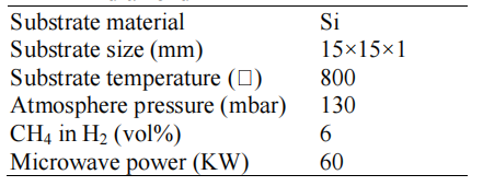
The polycrystalline diamond films were prepared by the microwave plasma chemical vapordeposition on silicon substrate. The growth parameters employed are shown in Tablel. The thicknessof the diamond film was 20 um, the arithmetic surface roughness (R,) was from 200 to 300 um, andthe maximum peak-valley height roughness (R) was 4-8um under the depositing condition (Table1.)

上一篇: 晶圆级封装的可靠性分析
下一篇: 晶圆键合制造技术回顾