ABSTRACT
The application market for Photonic ntegrated Circuits (PICs) is rapidly growing Photonic integration is the dominant technology in higbandwidth communications and is set to become dominant in many felds of photonics, just like microelectronics in the field of electronicsPICs offer compelling performance advances in terms of precision, bandwidth, and energy eficiency. To enable uptake in new sectors, theavailability of highly standardized (generic) photonic integration platform technologies is of key importance as this separates design fromtechnology, reducing barriers for new entrants. The major platform technologies today are Indium Phosphide (InP)-based monolithic integration and Silicon Photonics. In this perspective paper, we will describe the current status and future developments of InP-based genericintegration platforms.
1.INTRODUCTION: SIMILARITIES AND DIFFERENCESBETWEEN PHOTONIC AND ELECTRONICINTEGRATION
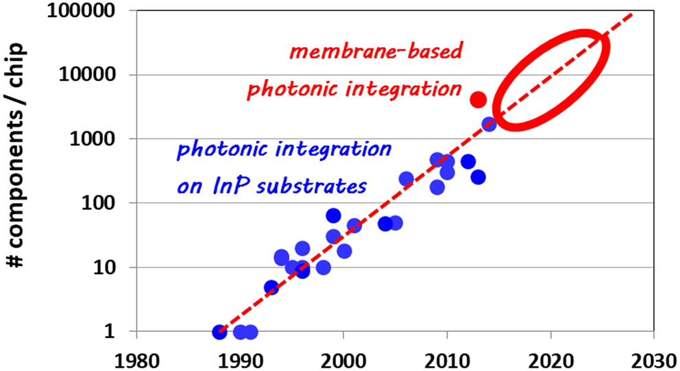
Already in the first publications on integrated photonicsknown at the time as “integrated optics”it was assumed that pho-tonic integration would follow the same path as microelectronicintegration (Miller, 1969, Tien, 1977). And indeed, we see a lot ofsimilarities. Figure l shows a clear exponential increase of photonicchip complexity (measured as the number of components integratedon a single chip), similar to Moore's law in electronics, albeit with aslightly smaller gradient (Smit et al, 2012).In the early years, significant research and developmentfocusedon the creation of the building blocks necessary for higher function-ality circuits. The arrayed waveguide grating (AWG) was a particularly important example of a circuit element enabling larger scaleintegration.
This de/multiplexing device enabled parallel circuit elements such as lasers and modulators to be combined to create wavelength multiplexed circuits, a technology which now underpins themodern internet. The blue dots in Fig. l show the advances in Pho-tonic Integrated Circuit (PIC) complexity enabled with the AWGTens of components were feasible at the start of the millennium and as integration with lasers and modulators has matured, hundreds of components are now being integrated. The most sophisticated circuits including lasers, modulators, detectors, and multi-plexers have more than 1000 components in one chip. One suchexample is a Terabit/second optical transmitter (Summers et al.,2014). With conventional Indium Phosphide (InP)-based integra-tion technology, it will be difficult to push integration levels muchhigher. However, in PICs where the light is confined in a thin mem-brane, such as silicon photonics, passive components can becomesmaller and higher integration densities are possible.
The high-est number of components per chip reported so far is 4096 for a64 x 64 phased array realized in Silicon Photonics (Sun et al, 2013),the red dot in Fig. 1. Component numbers per chip are now con-strained by electrical connectivity and thermal management. Mem-brane technologies, addressed in Secs. Ill and IV ofthis paper, offera route to the size and energy reductions required for higher den-sity integration, and for close integration with electronics, whichwill solve the interconnect bottleneck. In photonics, we do notforesee integration levels as presently achieved in digital microelectronics: physical dimensions and heat dissipation of photonic cir-cuits are orders of magnitude large than those of transistors. Inthis respect, photonics resembles analog and RF-electronics, where integration scales are also significantlylower than in digital electronics. However, when the present bottlenecks in heat management andefficient integration of photonic and electronic circuits are solvedwe expect that the exponential development can be pushed at least 2decades further.

Figure 1
A. Semiconductor integration technology
The production of wafer-based electronic and photonic tech-nologies have similarities as well as differences. Table I highlightssome of the milestones which have been reached in both electronicand photonic integration. The development of photonic and micro-electronic integration follows largely the same path, with a delayof 25 to 30 years for photonics, as indicated in Table I. The start-ing point for microelectronic integration was the invention of thetransistor (Bardeen et al, 1948; Shockley, 1948), a compact semi-conductor amplifier which replaced the bulky vacuum tubes. Thestarting point for photonic integration was the invention of thesemiconductor laser, which replaced the bulky gas and solid-statelasers (Alferov et al, 1969). In the early years, both the transis-tor and the laser were used as discrete components. In microelectronics, Kilby succeeded in 1958 to integrate a circuit containingseveral transistors in a silicon substrate (Kilby, 1958). In the earlydays, several technologies were explored, but in the 1970s CMOSbecame the dominant integration technology in microelectronics(Wanlass and Sah, 1963).In photonics, a first integrated circuit con-sisting of a laser integrated with a modulator was reported in 1987(Suzuki et al, 1987). The integration of several components in a semiconductor substrate marked the start of a long period ofexponential development, which we know as Moore's law.
上一篇: 硅上多晶磷化铟的生长和表征
下一篇: 晶圆级微光学制造