Abstract
Micro-optics is an indispensable key enabling technologyfor many products and applications today. Probably the mostprestigious examples are the diffractive light shaping elementsused in high-end DUV lithography steppers. Highly-efficientrefractive and diffractive micro-optical elements are used forprecise beam and pupil shaping. Micro-optics had a majorimpact on the reduction of aberrations and diffraction effectsin projection lithography, allowing a resolution enhancementfrom 250 nm to 45 nm within the past decade. Micro-opticsalso plays a decisive role in medical devices (endoscopes.ophthalmology), in all laser-based devices and fiber com-munication networks, bringing high-speed internet to ourhomes. Even our modern smart phones contain a variety ofmicro-optical elements. For example, LED flash light shapingelements, the secondary camera, ambient light and proxim-ity sensors. Wherever light is involved, micro-optics offersthe chance to further miniaturize a device, to improve its per-formance, or to reduce manufacturing and packaging costsWafer-scale micro-optics fabrication is based on technologyestablished by the semiconductor industry. Thousands ofcomponents are fabricated in parallel on a wafer. This reviewpaper recapitulates major steps and inventions in wafer-scalemicro-optics technology. The state-of-the-art of fabrication.testing and packaging technology is summarized.
1. Miniaturized lenses and array optics
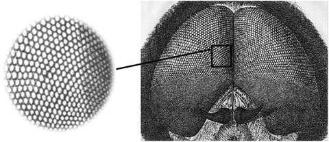
The first micro-optical elements were manufactured byAntonie van Leeuwenhoek (1632-1723), a pioneer of micros-copy and microbiology. Leeuwenhoek melted small rods ofsoda lime glass in a hot flame to obtain high-quality glass spheres. These ball lenses improved the resolution of hismicroscope viewers beyond current limits. He was the first toobserve and report on single cell micro-organisms. Anotherpioneer of microscopy, Robert Hooke (1635-1703), publishedhis famous book Micrographia, a collection of microscopeobservations, in 1665 [1]. Among them is the fascinatingdrawing of a fly's compound eye shown in Figure 1, a naturalmicrolens array.The first natural microlens arrays appeared very early inevolution some 500 million years ago, in the Early CambrianperiodTrilobites, a fossil group of marine arthropods, had com-plex compound eyes with microlenses made of calcite(Figure 2). Still today, similar compound eyes are found inmany small creatures. Microlens arrays seem to be the appropriate solution for miniaturized vision systems in nature.

Figure 1
2. Early inventors and microlens arrays
The development of planar diffractive and refractive microoptics is very much connected with photo- and cinematography. In 1891,Gabriel Lippmann (1845-1921) inventedinterference color photography’[2]. He fixed a mirror incontact to the photographic emulsion and recorded the interference pattern from incident and reflected light in a sensi.tive but transparent emulsion. The Lippmann color photoslater referred to as Lippmann holograms, were in fact the firstwavelength-selective volume holograms. For white light illu-mination, constructive and destructive interference generatecthe color image in reflection. This invention was made withoutlaser and long before Denis Gabor invented the holography in1948 [3]. Lippmann also invented integral photography, anauto-stereoscopic method to display three-dimensional (3D)images for observation with the naked eye [4].Integral photography uses an array of small microlenses torecord multiple sub-images of a scene in a photographic layer.Each microlens acts like a miniaturized camera recording anindividual sub-image. Observing the developed photo platethrough a similar lens array, the superimposed sub-imagesform an auto-stereoscopic integral image, a 3D image. In1912, Walter Hess [5] proposed to use an array of cylindricalmicrolenses as shown in Figure 3. These 3D displays basedon cylindrical microlens arrays were later referred to as paral-lax panoramagrams. Current 3D postcards and some current3D television screens are based on this principle.Another important field of applications for microlens arraysinclude the fly's eye condensers, also referred to as Kohlerintegrators.mination for color slideor fifi lm projectors. Figure 4 (right) shows a K ö hler integrator, consisting of two microlens arrays at a focal-length distance, for illumination of color fifi lm projectors, as proposed by Joseph Mihalyi in 1927 [6] . Similar microlens beam homogenizers are widely used in all types of illumination systems today [4, 7 – 9] .
3.The lack of a suitable fabrication technologyhinders innovation
Over the past 100 years, many researchers published and patented inventions, where refractive or diffractive array opticswas the decisive key element for light shaping or imagingOften brilliant ideas, but only a few could be realized andeven fewer were a commercial success. For early micro-optics applications, the insurmountable entrance barrier wasthe availability of suitable micro-optical elements at reason-able costs. n the early days, microlens arrays or grating wereengraved or polished, for example, on a lathe as shown inFigure 5.This piece-by-piece fabrication was very time-consumingexpensive and the arrays were not very uniform. Later, glassmolding, casting and pressing was used, for example, to man-ufacture fly's eye condensers for slide and film projections.Often, the quality of these microlens arrays remained poorSurface roughness, defects, lens profile accuracy and non-uniformities in the array constrained their field of applications.
上一篇: InP的光子集成的过去、现在和未来
下一篇: 碳化硅的化学机械抛光