Abstract.
With the advancement of semiconductor technology, the assembly processsemiconductor packaging is driving the devices to become smaller and smaller in size. One ofthe critical processes in backend assembly is the product's singulation to separate bulk processedproducts into individual unit. Before the sawing process kick-off, saw blade preparation (bladedressing) has to be performed. Blade dressing is the process of sharpening the saw blade surfaceto expose the diamond grits to the blade surface that are covered by the blade bonding materiaNickel-based). Inappropriate blade preparation technique induces burn mark defect tosemiconductor devices. This research presented the dressing process optimization on criticafactors using Silicon carbide (SiC) as part of the effort to enhance the product quality. The 2!Full Factorial Design of Experiment (DOE) methodology, with consideration of three factorsnamely Blade Revolution Per Minute (RPM), Feedspeed and Dress Pass. The overall singulationprocess yields performance improvement by reducing the burn mark to < 0.1% with optimumsaw blade preparation technique. Besides, the optimized process complementarily contributes toless kerf deformation and dressing wear.
Introduction
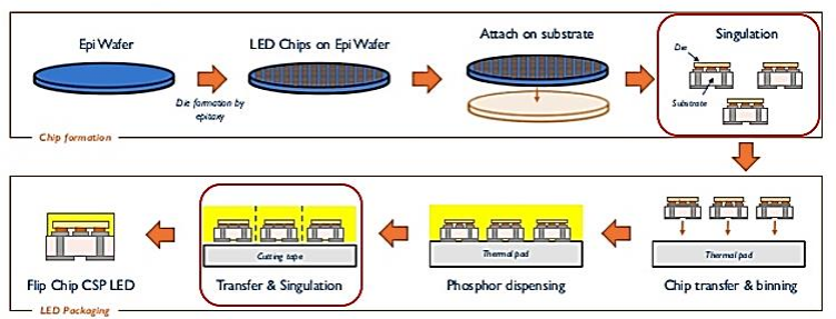
Electronic semiconductor industry has enjoyed consistent growth over the decades. In year 2017, theglobal electronic semiconductor market grew 21.6% according to the World Semiconductor TradeStatistic (WSTS). This industry growth was driven by two dominant factors which are the electronicproducts market pull and semiconductor electronic packaging technologies advancement and innovation(1]. This technology evolution has changed the products size to become smaller as Moore's Lawexplained this scenario well in claiming that, the transistor density doubles every three years.Numerous packaging technologies have been developed over the years, from individual diepackaging, dual in-line package, surface mount technologies, chip-scale packaging, to wafer levelpackaging and more complicated, 3D package integration, the svstem-in-package and package-on.package that established in 2000s. 2 . All these advanced technologies process semiconductors productsin bulk: hence. singulation process must take place to separate the products into individual partSingulation precision and quality are the essential criteria. One of the critical processes is the productssingulation during the typical opto-semiconductor (LEDs) packaging process as shown in Figure 1.which is the singulation process. It plays an important role in producing a defect-free and highly precise-dimension product.

Figure 1
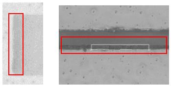
Before a sawing process kick-off to singulate semiconductors assembly parts into individual unitssaw blade preparation (blade dressing) have to be performed. Blade dressing is the process of polishingthe saw blade surface to expose the diamond grits to the outer layer that is covered by the blade bondingmaterial 3]. Optimized blade dressing recipe is critical to ensure the saw blades give perfect cuttingperformance and outcome on the semiconductors products.Inappropriateness in saw blade preparation technique induce burn mark at the contact area betweenthe devices and the saw blades. urn mark in semiconductor device as shown in Figure 2 considers asrejected unit as it is not only a cosmetic defect (as per most customers requirement) but also affects thefunctionality of the product, for example the emitter luminance in opto-electronic devicesApproximately 3.88% of burn mark defect rate observed in singulation process involved Film layerPhosphor-based material [4].

Figure 2
Advanced Packaging and Dicing Technology
The growth of the semiconductor electronic industries remains to be forcefully impacted by theworldwide major trends. The most significant impact on the semiconductor electronic industry is theintroduction and communalized of smartphone globally. Due to huge global interest and volumeincreased, major innovation of this industry directed by the evolution of smartphone. Besidesenvironmental awareness, health-care. automotive and connectivity industry are also the megatrend thatare impacting the evolution of semiconductor electronic industry.The package dicing or sawing process is a cutting process that separates assembly parts intoindividual packaged semiconductor device. The dicing process can be performed by mechanical saw oraser ablation.The area that has been cut away during sawing process is called sawing street (5 . Industrand market requirement of advanced dicing technology have driven the innovation of dicing technologyto laser ablation (6), stealth dicing 7 , multi-wire sawing (8 and plasma dicing (97 introduced by Disco(Japan) Corporation.
上一篇: 半导体封装基板材料技术趋势
下一篇: 氮化铝陶瓷的金属化