The electronics industry has developed dramatically over the past halfcenturv. primarily thanks to the semiconductorindustry. Today, with increasing demand for smartphones and tablet computers, further high-volume, high speed, low powerconsumption ISIs and smaller/thinner semiconductor packages are strongly required. Meanwhile, the technical challengesnyolved in further fine pitch design shift the focus to assembly technology, which is considered the core technology requiredo achieve high-volume, high-integration semiconductor packages. Recently, the market for 3D semiconductor packages such asPackage on Package (PoP), capable of stacking different IC packages such as memory and logic, is growing. Materials whichhave supported the development of such semiconductor packages include printed wiring board materials and semiconductorackaging materals.This renort wll introduce the historv oforinted wiring board materals and its technical trends in future
Introduction
The electronics industry started with the commercialization of transistors in the 1950s, and has since grown into a $45 trillionmarket. Since personal computers (PCs) were introduced in the market in the late 1980s, the Internet and cell phones havebecome ubiquitous, and smartphones and tablet computers are recently growing markets. Electronic components and materialshave supported the development of the electronics industry. apanese semiconductors and electronic devices account for 20% ofinternational markets. while the share of electronic components and materials exceeds 40%, reflecting the fact that the superiorityof lapanese high-function materials is aproved by the international community. The printed wiring board (PWB) is an electroniccomponent incorporated in electronics, and comprising printed wiring board materials. Hitachi Chemical has developed advancedelectronics technologies, and continuously marketed electronic materals that contribute to the electronic industry. This reportpresents the history, recent technical trends and future development of such printed wiring board materials.
What are Printed Wiring Board Materials?
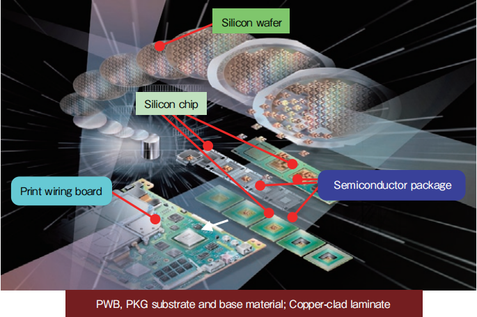
The role of PWB is to transmit electric signals to electronic components such as semiconductor silicon chips incorporatedinto electronic equipment such as computers via copper circuits. Figure 1 shows the hierarchical structure of silicon chipssemiconductor package substrates (“PKG substrates), and PWB. The printed wiring board materials, including copper-cladaminate (core materia), which is the base of PWB, photosensitive dry films for forming circuits and solder resist (Figure 2)compose the PKG substrate and PWB.

Figure 1
Evolution of PWB
PWB was mainly developed in the United States during the 1950s. The etched foil method featuring chemical etchingof copper foil on the substrate to formulate a circuit was mainly used for manufacturing PWB. In Japan, the first prototyppaper phenol copper-clad laminate was manufactured in 1954, and about half a century later, technology has evolved into masproduction of cutting-edge PKG substrates equipped with high Tg epoxy copper-clad laminates. These materials consist of acombination of a matrix layer of thermoset resin and basic material, and the structure is basically the same.Circuits are wired onto these copper-clad laminates using a photosensitive dry film to produce PWB. which is classifiecaccording to the concept of"generation" depending on the materials and structures’. Table 1 lists the generations and associatematerials. Due to evolution. PKG substrates are much denser than PWB. and a method known as a semi-additive process (SAP) imainly used for formulating circuitry.
上一篇: RCA清洁变量对颗粒去除效率的影响
下一篇: 半导体器件封装单片化工艺优化