Introduction
Solar cells applying heterojunction emitters of amor-phous silicon on a crystalline-silicon substrate havedemonstrated high efficiencies without requiring high-temperature processing. The performance of hetero-junction solar cells is improved by reducing defects atthe interface by inserting a very thin intrinsic a-Si layerbetween the doped p-type a-Si emitter layer and the ntype c-Si substrate.
The amorphous silicon is deposited on the texturedsurface. In between texturization and a-Si deposition acleaning is performed. This cleaning serves to removeany unwanted contamination that is present after thetexturing step, which is usually considered a dirtyprocess. A second function of the clean is to preparethe surface for the a-Si deposition. Usually the clean isterminated by a treatment in hydrofluoric acid (HF)This treatment passivates the dangling bonds at theinterface with hydrogen, thereby reducing the interfacestate density. It is generally expected that a good pas-sivation after cleaning is beneficial for obtaining agood passivation after amorphous silicon deposition.
In practice the cleaning may actually be split up in twoparts, each dedicated to contamination removal andsurface preparation respectively. Figure 3 shows anactual sequence of cleaning steps as it was used inImec. The goal of the current paper is to evaluate alter-native wet-chemical cleans in order to simplify thecleaning with equal or better performance.
Experimental
The substrates used in this work were p-type FZ sam-ples with a thickness of 200um and a resistivity of202.cm. Prior to the experiment, all samples received areference clean consisting of SPM + HF/HCl (for description of the cleaning steps, refer to Table 3).Some samples were intentionally contaminated by atreatment in KOH. In this study, the contamination wasassessed by means of Total X-Ray Fluorescence(TXRF). Because TXRF cannot be applied on rough(textured) surfaces, the samples were not actually tex-tured but dipped for a short period in the KOH solutionwithout significant etching. After the KOH treatmentthe samples were cleaned. For each cleaning processreference samples were included that were not treatedin KOH. Part of the samples was analysed by TXRFusing W-LB excitation. Other samples were passivated by 10nm intrinsic a-Si on both sides (deposition tem-perature 140°C). After a-Si deposition the minoritycarrier lifetime was measured using quasi steady statephotoconductance(OSSPC).
Results

Figure1
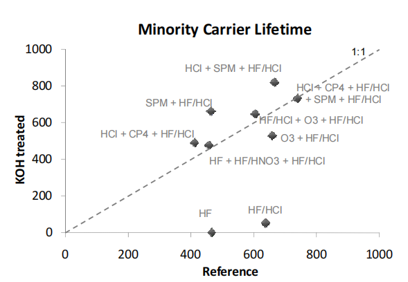
Figure 4 shows a comparison of the lifetimes that wereobtained on samples with different cleaning processesFor the majority of the results, the differences are con-sidered insignificant compared to the reproducibility ofthe experiment. However, in two cases, where thecleaning consisted only of immersion in HF or HF/HClmixture, the lifetime was particularly low on samplesthat received the KOH treatment.TXRF measurements show (Figure 5) that in mostcleans the metal concentration is reduced to below 1010at/cm?. Only for the two conditions where lifetime waslow, a significant amount of Cu was found.
上一篇: 石墨烯-半导体异质结对新兴光伏的研究
下一篇: 自清洁半导体异质结衬底