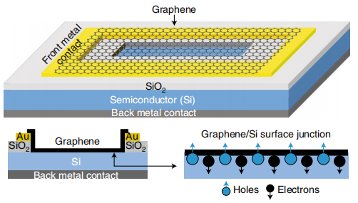
Electronic coupling of graphene atop a bulk semiconductor and the resultant interfacial energy-band reorganization create8ight-sensitive junction onlyone atom below the front surface. Uniquely, this architecture leads to the surface being in extremeilose proximity to the depletion region (typically buried several micrometres under the surface for a conventional waferp-n junction solar celD), thus providing direct access to the photosensitive junction, which can be modified by surface functioralization and/or incorporation of plasmonic nanoparticles, The surface-based heterojunction, tunable carier transportanorelatively enhanced optical absorption in such 2D -laver-interfaced 3D semiconductor svstems will have a transformative impaciin the field of 2D optoelectronics, photovoltaics, photonics and nanoelectronics.
Several unique functionalities of the 2D/3D device architecturehave emerged over the past decade with a sustained focus on het-erojunction photovoltaics and continued innovation in their surface/interfacial science, materials chemistry and device physics.Graphene or other optically transparent and active absorber 2Dlayers, including reduced graphene oxide, three-atom-thick semi-conducting transition metal dichalcogenides and two-atom-thickphosphorene, are interfaced with direct- or indirect-bandgap 3Dbulk semiconductors for photovoltaic phenomena. To establish thecharge-transport mechanism and to amplify the performance effi-ciency of such 2D-on-3D photovoltaics, several routes have beenemployed, including (1) chemical doping or surface functionaliza-tion of 2D layers (to tune the chemical potential and work function).(2) interfacing metallic nanoparticles on the 2D surface junction(to plasmonically boost the photon absorption and the short-circuitcurrent density (so)), (3) employing antireflection coating (ARC)layers (to optically manage the light absorption), (4) inclusion ofhole-transporting insulating 2D layers (to increase the surface-junction barrier, and with it the open-circuit voltage (Voc)), and(5) interfacing graphene or other 2D materials with Ill-V compound semiconductors.
Low-dimensional sp2 carbon materials for solar cellsFunctional 2D nanomaterials (2DNs) have shown great promisein optoelectronic applications?, including photovoltaic solar cells,photosensors, photodiodes and photodetectors. Graphene, a sp?hybridized carbon monolayer, has been extensively investigated forphotovoltaic energy conversion, owing to its robust in-plane intrin-sic strength, high charge-carrier mobility and relatively high opticaltransparency. The graphene layer has been employed for differentpurposes in the various generations of photovoltaic technologies:(1) transparent conducting film for amorphous silicon (Si)-based and indium gallium nitride (InGaN)-based solar cells', (2) activelight-harvesting material for Si-based heterojunction photovoltaiccells’,(3) counter cathode electrode for dye-molecule solar cells(4) photoanode electrode for organic solar cells, and (5) high-per-formance hole-transporting material for hybrid organic-inorganicperovskite solar cellss. Broadly, the graphene film has dual function-ality and is employed as a transparent conductor and as an atomi-cally thin photoabsorber sheet in the photovoltaic cells. Currently,doped metal oxides, including indium tin oxide and fluorine-dopedtin oxide transparent electrodes, are employed for charge injectionor collection in thin-film solar cells. These transparent conductiveoxide thin films are typically brittle (ceramic materials) and expen-sive (indium is scarcely available), which makes them unsustainablefor optoelectronic or photonic devices. In contrast, low-dimensionalsp?-hybridized carbon nanostructures, including fullerenes, carbonnanotubes and graphene, have been utilized as optically transpar-ent, electrically conductive and mechanically flexible electrodes inorganic-, polymer-fullerene- and dye-molecule-sensitized (Gratzelcells)-based solar cells.
In this Perspective, we focus on the concept of the surface junc-tion': the photojunction only one atom below the front surfacewhich is produced due to the interfacing of 2D layers (graphene)with bulk 3D semiconductors (Si). Here, graphene functions asboth a light transparent electrode and a charge-separating, transport-active layer. In these 2D/3D heterojunction-based emergingphotovoltaic cells, a light energy to electricity conversion efficiencyof 15-17% can be achieved with improved nanoarchitectures andcombined surface/interface engineering . Figure l shows a schematic of a graphene/semiconductor heterojunction and the charge-carrier transport across the angstrom-scale surface junction.

Figure 1
Energy-band structure engineeringTo enhance the performance of graphene-on-semiconductor heterojunctions in optoelectronic applications, a uniquely accessibleroute is to engineer the interfacial band structure to control theelectron- and hole-transport phenomena. For the heterojunctionsolar cell operation, the built-in voltage across the depletion regionof the surface junction (here, the 2D/3D heterojunction) playsan important role, as it not only drives the photoexcited charge carriers towards the contact electrodes, but also avoids chargecarrier recombination. Therefore, it is essential to understand thetransport of charge carriers, potential barrier formation, built-inpotential-induced band-bending at the junction, and the relation-ship between the performance of 2D sp?-carbon-based heterojunc-tion solar cells and the surface-junction characteristics.
上一篇: 快速扩大 GaAs晶圆背面处理的挑战
下一篇: 异质结太阳能电池纹理化后清洗的优化