Introduction Due to low production costs and decreased operating temperatures, plasma enhanced chemical vapor deposition (PECVD) remains the dominant processing method for the manufacture of silicon thin fifilms in both the solar cell and microelectronic industries [1–3]. Given the diffificulty of in situ measurements during the deposition of amorphous silicon thin fifilms, numerous groups have developed models to characterize the behavior of PECVD systems. Specififically, gas flflow and volumetric chemical reactions within PECVD reactors have been investigated using computational flfluid dynamics (CFD) models of varying complexities [4–6]. Additionally, the complex chemistry and surface interactions that defifine the microscopic growth of thin fifilm layers have been modeled [7–10] using kinetic Monte Carlo models and such models have been demonstrated to reproduce amorphous silicon fifilms with accurate growth rates and morphologies. Furthermore, signifificant efforts have been made in linking macroscopic fifirst-principals models of gas phase species concentrations and temperature employing approximate flflow fifield equations with microscopic surface models (e.g., Rodgers, S. and Jensen, K., 1998, Lou, Y. and Christofifides, P.D., 2003 and Aviziotis et al., 2016 [11–13]). However, macroscopic CFD models that develop an accurate flflow fifield solution without approximation and microscopic surface models have not been linked in the context of PECVD. Unfortunately, potentially decoupled CFD and surface interaction models are unable to capture phenomena which occur at the boundary (thin fifilm surface) between the two PECVD simulationdomains. One such phenomenon, which remains a persistent issue during the manufacture of amorphous silicon thin fifilms, is non-uniformities which develop in the thickness and morphology of deposited layers across the radius of the wafer. Spatially non-uniform deposition has been well characterized [14–16] and shown to affect the effificiency of solar cell products [17], resulting in poor device quality and increased costs [18]. As such, there exists a need for accurate PECVD reactor models which are capable of predicting the codependent behavior of the macroscopic gas phase and microscopic thin fifilm growth. Multiscale models of this type may provide insight into the root cause of spatial non-uniformities present in the deposition of silicon layers, as well as allow for improved reactor geometries and optimal operating strategies to be developed. To this end, a multiscale CFD model is proposed in this work which captures the interconnection between the macroscopic and microscopic domains in PECVD systems. This model is applied to the PECVD of a-Si:H thin fifilms at industrially relevant conditions of T = 475 K, P = 1 Torr and a 9:1 ratio of hydrogen to silane gas in the feed. At the macroscopic scale, a structured mesh containing 120,000 cells is used to discretize the chambered reactor geometry. ANSYS Fluent software is used as a framework to solve the governing momentum, mass and energy equations which defifine the dynamics of the process gas inside the parallel plate PECVD reactor, and to orchestrate the communication between simulation domains. Three user defifined functions (UDFs) are implemented in order to tailor the Fluent architecture to the specifific application of the deposition of amorphous silicon thin fifilms. The fifirst accounts for the 34 prevalent gas phase reactions, including nine ionization reactions which produce the plasma. A second UDF provides an accurate electron density profifile based on the work of Park et al. [19]. The fifinal and most computationally demanding function comprises a hybrid kinetic Monte Carlo algorithm used to model the complex surface phenomena which characterize the microscopic domain. Additionally, given the signifificant computational requirements of this work, a novel parallelization strategy is developed and applied to both the reactor mesh and the individual microscopic thin fifilm simulations. The model described above is applied to the batch deposition of a 300 nm thick a-Si:H thin fifilm. Spatial gradients are shown to develop in the concentration of SiH3 and H near the surface of the silicon wafer. Consequently, non-uniformities in the thin fifilm thickness and hydrogen content are predicted to exceed 20% and 3%, respectively. These results represent an unacceptable margin from a manufacturing standpoint and highlight the importance of multiscale models in predicting and characterizing the behavior of PECVD reactors such that improved reactor geometries and operating conditions may be achieved.
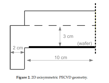
Process Description and Modeling The PECVD reactor utilized in this work belongs to the widely used subclass of CVD reactors known as chambered, parallel-plate reactors. The specifific geometry used in this investigation is a cylindrical reaction chamber with a 20 cm wafer capacity and 3 cm showerhead spacing (Figures 1 and 2). Process gases are pumped into the inlet at the top of the reactor before being distributed through circular showerhead holes into the reaction zone (light grey region in Figure 1). Within the reaction zone plasma is produced via a radio frequency (RF) power source across the parallel plate structure. The resulting plasma phase species flflow radially outward across the wafer surface, eventually exiting the reactor through outlets near the bottom. The specififics of the plasma chemistry will be provided in the macroscopic modeling section (Section 2.2 and Table 1 below). Two distinct simulation regimes may be specifified within the PECVD process: the macroscopic gas phase which can be described by momentum, mass and energy balances, as well as the complex, microscopic surface interactions that dictate the structure of the silicon thin fifilm of interest. Figure 1 highlights the multiscale character of this process and the need to capture the dynamics at both scales due to the codepedency between the macroscopic and microscopic regimes. The following sections detail both the macroscopic gas-phase model and the microscopic surface model.


上一篇: 2023年半导体项目
下一篇: 单片炉的设计及在快速热处理中的应用