Introduction
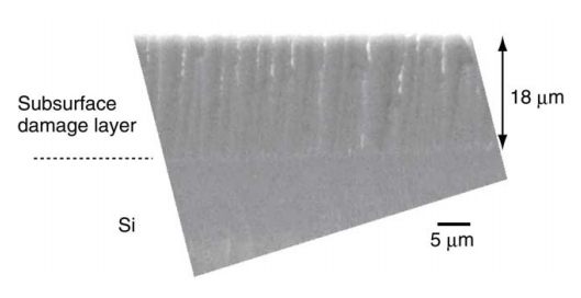
Three-dimensional (3D) integration using through silicon via (TSV) interconnects has been developed as an emerging technology that can lead to an industry paradigm shift. It can realize advanced high-speed, low-power, compact, and highly functional electronic systems by vertically stacking and connecting various materials, technologies and functional components (1-5). In the fabrication process of 3D integration, Si wafer thinning process is very important because it significantly affects the yield and the performance of 3D integrated circuits. Current Si wafer thinning is performed by the backgrinding using diamond wheels followed stress relief process (chemical mechanical polishing (CMP), dry polish, plasma etching etc.). Backgrinding has been recognized as an important wafer thinning process, owing to the high speed removal of Si and the ability to obtain high dimensional accuracy. However, previous studies demonstrated that backgrinding causes a subsurface damage layer (e.g., crystalline defects/dislocations and microcracks), which induces residual stress into wafer, and causes wafer/chip breakage or degradation of circuit component (6-10). Figure 1 shows an example of the intensely damaged region in Si wafer after backgrinding with 2000 grit diamond abrasive. Because the subsurface damage layer is very deep (18 μm), it is difficult to remove the subsurface damage layer completely by the stress relief process.
In order to overcome the technical issues of backgrinding, we proposed wet-chemical Si wafer thinning process (11,12). Figure 2 shows the process steps of wet-chemical Si wafer thinning. In this process, wafer thinning is performed by only wet etching of Siusing HF/HNO3 solutions. First, a Si wafer is clamped by a Bernoulli chuck system or vacuum chuck system. Next, spin etching of Si is performed using the solution which comprises HF and HNO3. Then, the spin rinsing with water is performed for surface cleaning. Finally, spin drying is performed. In the previous study, we demonstrated a high etching rate (around 800 μm/min) (Figure 2) and a uniformity of ±3% for the etched amount (in 6-8 inch wafers) by optimizing the component ratio of the solution. This study aim to evaluate the damage caused by wet-chemical Si wafer thinning process and to demonstrate wet-chemical Si wafer thinning process offers high chip strength.

Figure 1. An example of the intensely damaged region in Si wafer after backgrinding with 2000 grit diamond abrasive. The depth of subsurface damage layer can exceed 10 μm and hence perfect removal of subsurface damage is difficult.
上一篇: 用于高密度晶圆互连的微加工晶圆减薄
下一篇: 用于晶片到晶片堆叠的硅减薄工艺的表征