Abstract ¾ Thinning of micromachined wafers containing trenches and cavities to realize through-chip interconnects is presented. Successful thinning of wafers by lapping and polishing until the cavities previously etched by deep reactive ion etching are reached is demonstrated. The possible causes of damage to the etched structures are investigated. The trapping of particles in the cavities is studied and cleaning procedures are developed to address this issue. The results achieved so far allow further processing of the thinned wafers to form through wafer interconnections by copper electroplating. Further improvement of the quality of thinned surfaces can be achieved by alternative cleaning procedures. Keywords ¾ wafer thinning, lapping, chemical-mechanical polishing, through-wafer interconnects
I. INTRODUCTION High dense three-dimensional (3D) integration is achieved by extending the 2D integrated circuit to the vertical direction [1-4]. Hence, it results in high increased density with reduced volume, and the interconnection dramatically shortened which can significantly improve the performance for high speed, low power dissipation. Through-chip interconnections are an essential aspect in the realization of high dense three-dimensional integration, RF (radio-frequency) MEMS (micro-electro-mechanical system) structures and microsensors packaging. Thinning wafers is an important part of the process to achieve high-density, closely spaced interconnects. Specifically thinning of wafers with micromachined structures such as deep trenches, vias or cavities in order to obtained well-defined and controlled through-wafer holes, is a challenging step.
Several methods, chemical or mechanical, can be used to address this challenge. When using a chemical thinning method two approaches can be followed. The first one consists of forming a cavity from the backside followed by deep dry etching from the front side. The other is to first etch the deep vias or trenches and to perform chemical etching from the backside until the bottom of these etched cavities is reached. In both approaches the thinning down of the wafer is done using wet etching processes that are often slow and crystal orientation dependent. Another method, which might be more attractive for modern high-density electronics is to use mechanical thinning (lapping or grinding) followed by a chemical mechanical polishing process. With this method multiple chip stacks, and quite compact systems can be realized. However, there are several problems related to mechanical thinning, especially in the case of micromachined wafers. For example, mechanical damage to holes or trenches during lapping can occur. The presence of etched cavities can result in inhomogeneous distribution of pressure under certain load, leading to a variation of thinning speed or causing internal stress near the cavity edge negatively impacting and damaging components present in or around the cavities. Finally, during the grinding or lapping and chemical mechanical polishing, a lot of particles are generated. These particles might be trapped in the through wafer holes or trenches and if these particles can not be removed, further process of the wafers after thinning will not be possible.
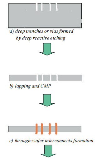
In this paper, mechanical thinning of the wafers with micromachined structure is investigated. The aim is to build complete 3-dimensional structures, including through-chip interconnections, as schematically shown in figure 1. After deep dry etching of trenches of via at the front side, the wafer thinning is then performed from the backside by lapping and chemical mechanical polishing. After wafer thinning Cu electroplating is employed to form through chip interconnections. The behavior of the cavity structures during thinning is also investigated.

II. EXPERIMENTAL Boron doped, p--type (100)-oriented silicon wafers with a resistivity of 2-5 W×cm and a thickness of 525+/- 25 mm, are used in our experiments. A 3 m m-thick PECVD oxide is deposited onto the silicon front side to serve as mask layer for the deep silicon etching. A mask containing vias, trenches and cavities of different sizesand shapes is patterned in the oxide. The deep vias and trenches are etched using induced couple plasma (ICP) in a SF6 /O2 gas mixture. Two different equipments and processes are used depending on the required depth. For cavities up to 100m m in depth, a Trikon Wmega etcher with a substrate temperature set point of 10° C is used, while for deeper structures or more anisotropic profiles an Alcatel ICP etcher and a substrate temperature of - 120° C is employed. After the silicon etch step the mask oxide is stripped. A l-Logitech LP50 lapping and polishing machine is used for the mechanical thinning. To handle the wafer during lapping and polishing, the test wafers are either directly attached to glass by anodic bonding or glued to another handle wafer with wax. The lapping is performed using a 9m m Al2O3 slurry. As much as 400m m of bulk silicon can be removed in this first step. Further thinning of the wafer to the desired final thickness is done with a smaller particle size (3m m) Al2O3 slurry. Finally, chemical mechanical polishing with a 0.3m m-silica slurry (pH~10) is performed.
上一篇: 磷化铟晶片的研磨减薄
下一篇: 用于高芯片强度的湿化学硅片减薄工艺