InP wafers of 2 in. diameter have been successfully ground to a thickness of 100 ~m by mechanical grinding with cuptype diamond wheels. This process can be applied, for the first time, to the mass production of InP optoelectronic devices, similar to the technology for GaAs devices based on the wafer-rotating downfeed grinding method. The phenomena occurring in the grinding of InP were similar to those of GaAs, such as a rapid transition between mirror grinding and rough grinding, and a large wafer bow. However, the deformed layer due to the grinding of InP was discovered to be thicker than that of GaAs, because InP is a little more fragile. Still, it was thin enough, less than 1.5 ~m, to be eliminated by slight chemical etching. The finished surface roughness in mirror grinding was also greater, but 0.15 ~m Rmax was obtained with 3 ~m diamond grains, which is small enough to be applied in device fabrications.
InP wafers of 2 in. diameter have been successfully ground to a thickness of 100 ~m by mechanical grinding with cuptype diamond wheels. This process can be applied, for the first time, to the mass production of InP optoelectronic devices, similar to the technology for GaAs devices based on the wafer-rotating downfeed grinding method. The phenomena occurring in the grinding of InP were similar to those of GaAs, such as a rapid transition between mirror grinding and rough grinding, and a large wafer bow. However, the deformed layer due to the grinding of InP was discovered to be thicker than that of GaAs, because InP is a little more fragile. Still, it was thin enough, less than 1.5 ~m, to be eliminated by slight chemical etching. The finished surface roughness in mirror grinding was also greater, but 0.15 ~m Rmax was obtained with 3 ~m diamond grains, which is small enough to be applied in device fabrications.
Grinding Technology Grinding has been generally used as a wafer-thinning technology in the Si field, because of its excellent manufacturability. On the other hand, it was previously deemedunsuitable for compound semiconductor wafers because it inflicted considerable damage upon the ground surface. In the case of GaAs, the brittleness, which seems to be most troublesome in a mechanical grinding process, provides a valuable advantage in manufacturing; the very thin.

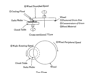
Fig. 1. Schematic view of wafer rotating downfeed grinding method. (a) Cross-sectional view, (b) top view.
0.6 ~m deformed layer can be easily removed by slight chemical etching (5). Such a thin deformed layer can be obtained only by the wafer-rotating downfeed grinding method, in which a high-speed rotating wafer is ground by the continuous downfeed of a cup-type diamond wheel whose grain size is either 12 ~m for rough grinding or 3 ~m for mirror grinding. A schematic view of this method is shown in Fig. 1. This method has a constant grinding force, because the contact area between the diamond wheel and the wafer is constant during the entire processing. In the present investigation, we applied the wafer-rotating downfeed grinding method to an InP wafer for the first time. After some modifications of the diamond wheel and grinding condition as shown in Fig. 1, an InP wafer was able to be ground with a very low frequency of wafer fracture. The ground surface roughness, grinding speed, wafer bow, and thickness of deformed layer were then examined and compared with GaAs and Si.
Ground Surface Roughness Experiment and results.--First, the ground surface roughness, Rmax, was investigated. Rm~x is the value which represents the degree of surface roughness, the difference between the highest and lowest points on the surface. Rmax must be approximately 0.1 ~m in order to get a strong die attachment and high thermal conductivity for InP-based electronic devices as well as GaAs ones, which are assembled by Au-Su eutectic bonding. As with GaAs, diamond grain size has a greater influence upon the surface roughness than other grinding conditions, such as wafer-rotating speed, wheel downfeed speed, and wheel peripheral speed9 The relation between surface roughness and grain size of the resin-bonded diamond wheel was carefully examined with respect to the boundary between the rough- and mirror-ground surfaces. The results for InP and GaAs are shown in Fig. 2 and are very similar to each other, for example, the rapid transitions between mirror grinding and rough grinding. However, there are two minor differences. One is that the rapid transition for InP occurs in a larger grain size (12 - 18 ~m) than that for GaAs (6 ~m). The other is that the Rma x of the InP ground wafer significantly improves as the grain size becomes smaller in the mirror grinding mode, while that of the GaAs wafer is slightly improved. In the following experiments, a diamond wheel with 3 ~m grains was used for mirror grinding, and with 18 ~m grains for rough grinding9
上一篇: 通过晶圆减薄提高 WL-CSP 的可靠性
下一篇: 用于高密度晶圆互连的微加工晶圆减薄