Abstract
WL-CSP is a low profile, true chip size package that is entirely built on a wafer using front-end and back end processing. The wafers can be batch-processed in a fab, which reduces the number of materials and packaging steps, reduces inventory, and allows for wafer level burn in and test. This technology is driven by cost, size, and ease of testing and is ideal for low to mid I/O devices. Peripheral bondpads from the die are redistributed into an area array using a photodielectric and a redistribution metal, eliminating the need for a substrate or interposer. Solder balls are placed onto the redistributed metal bondpads and reflowed, creating a large standoff which improves reliability. The bump structure and pad geometry of the test vehicle was optimized using simulation and validated by experimentation. This WL-CSP technology was evaluated using a 5 x 5 mm2 die with a 0.5 mm pitch 8 x 8 array of solder bumps. Board level reliability was performed using 1.2 mm thick, 2-layer FR-4 boards with 0.25 mm non-soldermask defined copper pads coated with OSP. Standard thickness WL-CSP wafers are 27-mils. An evaluation was performed to evaluate the potential reliability improvement of WL-CSPs by thinning the wafers. Wafers were thinned down to 4-mils thickness using two techniques. The first method is standard wafer backgrinding. The second is the novel approach of plasma etching, which results in a damage-free surface and improves wafer and die strength. Board level reliability will be presented comparing standard WL-CSPs to those thinned using the aforementioned techniques.
Introduction
As electronic components continue to shrink in size, the semiconductor industry is moving toward IC miniaturization. Wafer level chip scale packaging (WL-CSP) is becoming a popular method of packaging low to mid-I/O devices. WLCSP is cost effective, easy to test, and has a small footprint and low profile. Cost is a major factor driving WL-CSP technology. Wafer level packages are built entirely using fab-type batch processing at the wafer level, decreasing cost. Packaging steps are reduced because WL-CSP does not require materials and processes such as underfill, substrates, or interposers, which are typically found in chip scale packages (CSP) or ball grid array (BGA) packages. Packaging time and inventory can be subsequently reduced because WL-CSPs do not need to be sent to assembly houses. Wafer level burn-in and test (WLBT) is another driving force behind WL-CSP technologies. Test will no longer need to be performed prior to packaging. Once the wafer hascompleted the final packaging step, it can be burned-in and tested for known good packages (KGP). Testing at the wafer level reduces the number of test steps and requires less test capital thereby reducing costs by as much as 50%. Size is the third major driving force for wafer-level packaging. The footprint and profile of a WL-CSP is the same as the die. Motorola’s approach to WL-CSP technology uses redistribution at the wafer level, which replaces use of an interposer. Solder balls are placed at the wafer level to form first and second level interconnects. Package and board
level reliability results for this WL-CSP structure have been reported previously 。
Wafer Thinning
There are several benefits to thinning wafer level packages. Thinning the die can benefit IC components in several ways: by reducing thermal resistance, improving device performance, increasing reliability, and lowering overall package height so end application such as cell phones can be thinner. The focus of this paper is to evaluate the improvement in reliability by wafer thinning. Thinning the wafer helps to minimize die stress, which occurs due to mismatches in the coefficient of thermal expansion (CTE) between the silicon die and the board materials. The thinner die has less shear forces acting on it. The solder joint reliability is thus improved since the reduction in die stress allows it to flex with the board [2]. WL-CSPs thinned via mechanical back grinding and plasma etching are evaluated here. In typical mechanical grinding, unwanted silicon is removed from the backside of the wafer using a two-step process – coarse grinding followed by fine grinding. This is performed using a grinding tool that contains diamond particles of specific dimensions held by a bonding material such as epoxy, wax, or ceramic. During coarse grinding, typically 90% of the back grind is completed, significantly reducing the thickness of the wafer. Coarse grinding will cause microcracks and damage the silicon lattice. Fine grinding completes the back grind process and removes part of this damage, but still leaves some silicon flaws behind [3]. Plasma etching is a dry etching technology that uses atmospheric downstream plasma (ADP). Using this method, a wafer can be uniformly thinned without generating microcracks or damage to the silicon lattice. Plasma etching may be used after mechanical grinding to help remove surface defects created during the process. In ADP etching, an inert thermal plasma is generated by DC discharge at atmospheric pressure. The wafer is suspended in a chuck with thebackside facing down (in which there is no contact between the wafer and holder). Two electrodes directed upwards, at a 90° angle to each other, sit below the wafer. A plasma arc is formed when a DC field is applied between the two electrodes. Reactant is injected to the plasma stream, which uniformly etches the backside of the wafer 。
Test Vehicle
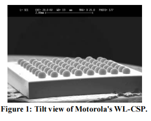
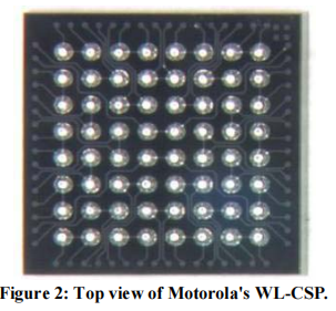
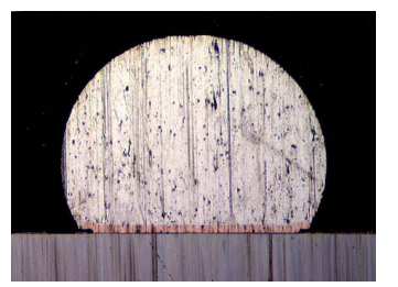
The test vehicle evaluated by Motorola is a 5 × 5 mm die with a 0.5mm pitch 8 x 8 array of solder bumps. Each six-inch wafer yields 496 packaged die. Photographs of the diced WLCSP are shown in Figures 1 and 2. Peripheral bondpads from the die are redistributed into an area array using sputtered aluminum redistribution metal with 300-um redistributed bond pads. The BCB redistribution photodielectric was 5 µm thick with 250 µm diameter openings to the bondpads. This redistribution process has been described previously [6]. The preformed solder balls were eutectic Sn-36Pb-2Ag with 300 mm diameter to give maximum bump height for the 0.5 mm pitch array. Figure 3 shows a cross-section of a WL-CSP.


Figure 3: Cross-section of the SnPbAg WL-CSP.
上一篇: 湿法刻蚀三维集成电路硅片减薄技术
下一篇: 磷化铟晶片的研磨减薄