INTRODUCTION
Semiconductors have been miniaturized by applying Moore’s Law. However, developments toward miniaturization remain issues of drastic increase in complexity and huge facility cost. On the other hand, techniques other than those for miniaturization have been implemented into developments of high-performance semiconductors. The most promising technique for developing high-performance semiconductors is of three-dimensional integrated circuit using silicon wafer (or chip) thinning and through silicon via (TSV). This technique offers the following benefits for high-performance semiconductors: (1) Increased memory capacity in a particular physical volume; and (2) Faster transmission speed and lower power consumption due to improved responsiveness between the logic and the memory resulting from thinning and TSV. In conventional thinning of silicon wafers, back grinding (BG) has been applied where the backside of a wafer is mechanically ground with a grindstone. However, the back grinding causes micro cracks/grinding traces on the back surface layer of the wafer or defects/damage inside it, resulting in reduced yield and mechanical strength of the wafer. As such, full wet process etching is necessitated for thinning silicon wafers, where only wet etching is used for all thinning processes in order to avoid such adverse effects on wafers caused by grinding. We already indicated the potential of this technique. [1] Wet etching of silicon wafers is roughly divided into two types depending on chemical solutions used, or acid and alkali, and the variation in characteristics of the chemical solutions differentiates applications of wet etching. The etching using the acid chemical solution uses such a solution of mixed HNO3 and HF as the basis. Silicon etching using mixed acid is reported as taking the two-stage reaction of Si oxidization by HNO3 and SiO2 dissolution by HF, as expressed in the following equations (1) and (2).
2. WET ETCHING RATE OF SILICON WAFERS WHEN USING MIXED ACID
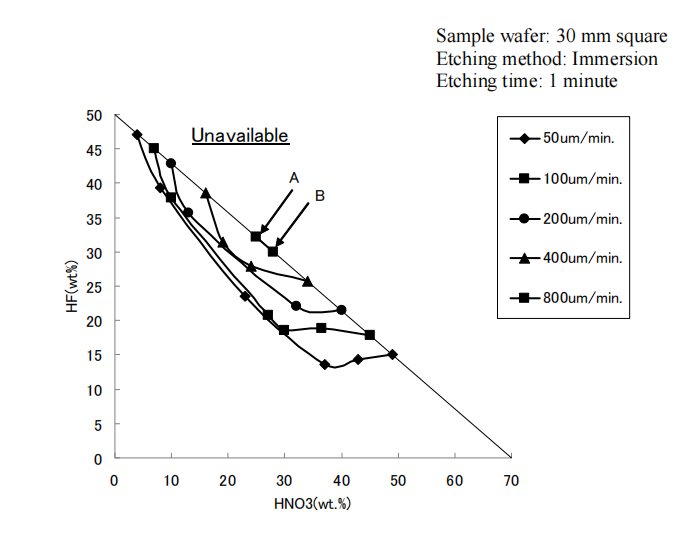
2.1. Method of experiment For the experiment to identify the etching rate, we used p-type silicon wafers shaped in about 30 mm square and 775 m thick. Mixed acid chemical solutions with different components of HNO3, HF and H2O were prepared by mixing HNO3 (70 wt%) and HF (50 wt%) commercially available and poured into beakers in which sample wafers were immersed for etching. The immersion was for one minute. The samples were oscillated in the solutions at a rate of 1.5 seconds per reciprocation. The etching rate was defined as an etched amount on one surface in one minute. The thicknesses of the sample wafers were measured before and after etching operation and the difference of the measurements were divided by 2 to determine etching rates.

Figure 1 contour map of etch rate in mixed acid solution.

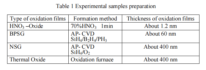
2.4. Experiment and discussion Tables 3 and 4 show etching rates of various oxidation films and their selectivity ratios to the thermally oxidized membranes calculated from the etching rates. The selectivity of the thermal oxidation film to HNO3-Oxide of [1:3] in the water solution exhibited an extremely large difference compared to that of [1:24] in the IPA solution. This result indicates that thermal oxidation film cannot be etched while there is reactive species possible to etch HNO3-Oxide. The HF2- concentration in the IPA solution used for this experiment was significantly smaller (1: 0.03) than that in the water solution; however the HF concentration was virtually the same. This result indicates that reactive species possible to etch HNO3-Oxide in the IPA solution is considered neutral HF. Also, HNO3-Oxide is considered not in a perfect SiO2 state.
上一篇: 切割技术对薄硅强度性能影响的研究
下一篇: 通过晶圆减薄提高 WL-CSP 的可靠性