Abstract
Thin silicon offffers a variety of new possibilities in microelectronical, solar and micromechanical industries, e.g. for 3D-integration (stacked dies), thin microelectromechanical packages or thin single crystalline solar cells. The wafers in this investigation were thinned back by grinding and subsequent spin etching steps for stress relief followed by separation into single test dies by sawing or etching. In order to characterize and optimize relevant process steps in terms of quality and fabrication yield, the mechanical properties were investigated considering the defect formation and strength. In this paper the inflfluence of three difffferent dicing technologies on the mechanical strength of thin silicon samples was investigated by 3-point bending tests. Sawing, Dicing-by-Thinning with sawn grooves and Dicing-byThinning with dry-etched trenches were used as dicing technologies. Analytical and numerical calculations were performed to calculate fracture stresses from fracture forces in 3-point bending tests taking into account the non-linear relationship of force and displacement during testing. Thus the fracture stress as a parameter of strength could be calculated for all tested samples. The results were statistically evaluated by the Weibull distribution based on the weakest link theory. This approach allows a more comprehensive understanding of the inflfluence of the process on strength properties independently of geometric factors. Samples, being separated by ‘‘Dicing-by-Thinning’’, have much higher strength than simply sawed samples. If trenches are fabricated by dry-etched process the strength can be increased tremendously.
Introduction
Within the last years back side thinning of fully processed product wafers has become a widely used technique in semiconductor industry. Steadily increasing demands for extremely low package height in the case of chip card ICs and the requirement for increased electrical performance of power semiconductors and high frequency devices are strong driving forces for the development of thin wafer technology. The thin silicon dies are fabricated by wafer back thinning technologies like grinding, polishing or etching; and wafer dicing technologies like sawing, Dicing-byThinning or laser cutting. Further demands are coming up when mechanically flflexible electronic systems are to be developed. One application can already be foreseen today: the integration of ultra-thin and bendable ICs in a roll-to-roll manufacture process. However, in order to derive a reliable flflexible electronic product (Fig. 1), detailed investigations of the strength and deformation of ultra-thin silicon samples have to be performed. If the mechanical properties are known, technology steps can be characterized and optimized. To characterize difffferent technology steps various testing methods can be used. For example, the ball on ring test is used to characterize the inflfluence of back thinning processes like grinding, polishing or etching on the strength [1] whereas。

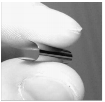
Fig. 1. Demonstration of flflexibility of 25 lm thin silicon chips prepared according to ‘‘Dicing-by-Thinning’’ concept using plasma etching for chip separation.

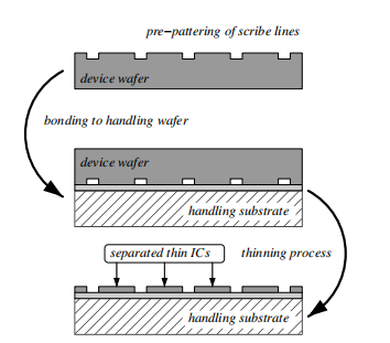
Fig. 2. Schematic process flflow according to ‘‘Dicing-by-Thinning’’ concept for preparation of ultra-thin silicon samples.
上一篇: 金属蚀刻残留物对蚀刻均匀性的影响
下一篇: 湿法刻蚀三维集成电路硅片减薄技术