INTRODUCTION
For fabrication of state-of-the-art complementary metaloxide semiconductor devices, high precision etch processes need to be developed. The size of structures that need to be etched is reaching less than tens of nanometers and the tolerances in the deviation from the target line width for etching of millions of features across 300 mm wafers is only a couple of nanometers. Moreover, the number of different materials, which are involved in device fabrication, is steadily growing. This requires an increase in etch steps and an increase in the complexity of etch processes in general. One parameter that can have a dramatic impact on the reproducibility of etch processes has been shown to be the composition of the etch chamber wall.1–4 This is especially true for low pressure 5–80 mTorr , high density inductively coupled plasma electron density 1011 cm−3 etch applications and the phenomenon can be explained by the fact that atomic species from the plasma can recombine to molecules on the chamber walls. The recombination can be so effective that it becomes a much larger loss mechanism for certain plasma species than the pumping of those species and thus it can have signifificant impact on the overall species densities in the plasma. Moreover, next to the overall species density also the uniformity of etch species in the plasma can be compromised. Certainly for large substrates, e.g., 300 mm Si wafers, the recombination of etch species on the chamber walls can lead to nonuniformities across the wafer. In the past, the impact of silicon and carbon based wall deposits on plasma etching has been investigated. In order to obtain reproducible plasma etch conditions, strategies need to be implemented to remove silicon or carbon from the walls or to condition the chamber so that it can deliver reproducible results. For example, dummy wafers can be etched to bring the chamber in the optimal condition seasoning , cleaning plasmas can be ignited after every processed wafer wafer less autoclean , or even coatings can be applied in the chamber before etching of each substrate. Nowadays, however, with the introduction of new materials, mostly metals, there are much more kinds of deposits that can form on the etch chamber walls besides silicon or carbon. These deposits each require special cleaning chemistries or strategies5 and therefore it was considered to be important to make an assessment about the impact of metal deposits such as Ti or Ta on different etch plasmas. Special focus was put on tantalum deposits because stable tantalum oxides are not removed from the chamber walls in a standard waferless autoclean process SF6 /O2 . Thus tantalum deposits are among the most prone to affect reproducibility in etch chambers. Clean and precontaminated chamber walls have beenused for O2, SF6, Cl2, and HBr plasmas and the impact of the walls on recombination processes has been studied through monitoring of O, F, Cl, and Br densities. This allows estimating recombination coeffificients for each of these species on the metal deposits. Especially for flfluorine and oxygen, these data are lacking in literature and are provided in this article. Additionally, experimental results are given to show the impact of recombination processes on etch rate uniformity across 300 mm substrates.
EXPERIMENT
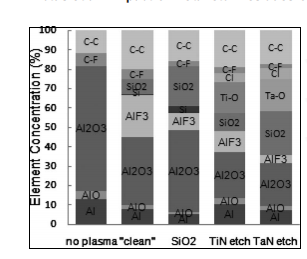
The experiments were carried out in an inductively coupled plasma etching reactor Lam Versys 2300 TCP , which is designed for etching 300 mm substrates. The plasma is excited by a 13.56 MHz planar spiral coil, which is separated from the plasma chamber by a quartz window. The wafers are electrostatically clamped to a chuck, which can be powered separately in order to accelerate ions to the substrate. This chuck also allows the wafer to be helium cooled so that it stays at approximately 60 °C during plasma treatments. The chamber walls exist of anodized aluminum and are kept at 60 °C during all experiments. The ratio of the total area of exposed alumina surfaces to quartz ware surfaces in the reactor is roughly 3/2. Before each experiment, the exact composition of the chamber wall is analyzed by the so-called flfloating sample technique developed by Joubert et al.6 During the cleaning process of the chamber or during the sputtering of contaminants on the chamber walls, a small Si wafer piece 2 2 cm2 is glued on a full wafer with a spacing of about 5 mm so that it is electrically isolated from that wafer. Since it is isolated from the wafer, it is only bombarded with ions with low energy. The plasma potential is 10– 15 V, so the ion energy of ions hitting the flfloating sample is maximum 15 eV and not hundreds of eV like the ions that bombard the wafer itself. The flfloating piece is at flfloating potential and behaves in that sense more or less like the grounded chamber walls.7 The deposits on this wafer piece are thus considered to be representative for the deposits on the chamber walls. The flfloating Si wafer piece has a top coating of 3 nm Al2O3, which is prepared by plasma oxidation of an aluminum layer on the silicon wafer.

FIG. 1. XPS analysis of flfloating wafer pieces that reflflect the condition of the etch chamber wall after different treatments.

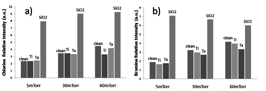
FIG. 2. a Relative Cl 808 nm intensities for different etch chamber wall conditions. b Relative Br 834 nm intensities for different etch chamber wall conditions.
上一篇: 硅片减薄集成工艺
下一篇: 切割技术对薄硅强度性能影响的研究