Abstract
A low cost and reliable wafer thinning process for Through Silicon Via (TSV) based three dimensional system in packaging (3D SiP) technology is presented. Silicon wafers were first thinned by means of coarse mechanical grinding with a mesh size of approximately #325, followed by fine mechanical grinding with a mesh size of approximately #2000. When applying a high feed rate to achieve higher material removal rate during the coarse grinding process, the thinned silicon wafer with edge crack was observed. It revealed that the stress on wafer edge contacting with grinding wheel was much larger than those at other locations. Mechanical grinding generated wafer warpage because of damaged layer created during the grinding process. Several stress release treatments, including chemical mechanical polishing (CMP) and dry etching process (plasma etching), were employed to thin silicon wafer and remove the damaged layer. The CMP and dry etching process can remove most of the damage produced by coarse and fine grinding, recovering both the mechanical strength and wafer warpage to their original status and resulting in a smoother surface
.Introduction Through Silicon Via (TSV) fabrication consists of five major processes: via formation, via filling, wafer thinning, wafer handling, and die/wafer bonding [1, 2]. Wafer thinning is one of key TSV processes which contributes more than 20% of TSV manufacturing cost and should be studied in a systematic manner. One fact of wafer thinning is that all the state-of-the-art thinning methods always leave a damaged layer on the thinned surface. The impact of the damaged layer to the mechanical properties of the thin wafer has been the topic of continuous research efforts [3, 4]. One of the major benefits of thin silicon devices is that they can enhance device performance and enable innovative packages for various applications. Based on current developments, the thickness of thinned wafers will start to approach 30-50 microns (um). Therefore, it is not surprising that silicon thinning and stress relief have become significantly important issues in the backend and assembly areas of semiconductor component manufacturers [5]. In this paper, a low cost and reliable wafer thinning process for TSV applications is presented. Silicon wafers were first thinned by means of coarse mechanical grinding with a mesh size of approximately #325, followed by fine mechanical grinding with a mesh size of approximately #2000. Several stress release processes, including chemical mechanical polishing (CMP), and dry etching, were used to thin silicon wafer and remove sub-surface damage caused by grinding. An integrated process used for silicon wafer thinning was given. Using the integrated process, 4 inches silicon wafer was successfully thinned to 30 microns
Experiments In the wafer thinned to 85um process, wafers are first thinned by means of coarse mechanical grinding with a mesh size of approximately # 325, followed by fine mechanical grinding with a mesh size of approximately # 2000. During grinding, deionized water was used to cool the grinding wheel and the wafer surface. After the fine grinding process, some stress/damage still remains in the sub-surface of the silicon wafer, which can induce wafer warpage. In order to reduce the stress so that wafer strength is increased and wafer level warpage is reduced, a form of stress relief becomes necessary. Several stress release processes including chemical mechanical polishing (CMP), and dry etching were used to thin silicon wafer from 85um to 30um and remove subsurface damage caused by grinding. The slurry, which was based on an alkaline solution with colloidal silica abrasive particles and an amine (NH3) additive, was used for the CMP process. In order to investigate etch rate of silicon when applying dry etching with different process condition, we used (111) oriented silicon as etch samples. The ICP (Inductively Coupled Plasma) equipment used is a standard load-lock system (Oxford Plasma lab system). Silicon samples with 1× 1cm2 size were mounted using a thermal conductive paste on a support wafer, which was held to an electrostatic chuck and was backside cooled using a water-flow cooling system. A mixture of SF6/O2 gas chemistry was used for the etching experiment. The influences of SF6 concentration in SF6/O2 gas chemistry and operating pressure on etch results were studied separately while other process parameters remained unalterable. The surface morphology and surface roughness were measured on silicon sample using atomic force microscopy (AFM). To determine the etch rate of silicon, the positive photoresist (PR) AZ4330 was spin-coated onto the silicon sample. After spinning, the wafer was soft-baked on a hotplate at 900 C for 90s, and the function of this step was to drive off most of the solvent and to establish the exposure characteristics. The wafer was then exposed and developed. A pattern was defined in the PR layer after exposure. During the develop process, the alkaline developer NaOH was used. After develop, the wafer underwent a hardbake on the hotplate at 1050 C for 270s, and the hardbake was used to harden the PR against further energetic process such as plasma etching. Finally, the pattern was transferred from PR into the silicon layer by using ICP etching. The average etching depth of silicon was obtained from the Detak stylus profilometry after the PR mask was stripped away. In order to obtain average etch depth, measurements of four different points on the silicon surface were performed. The etching rate was determined by the etching depth and etching time..

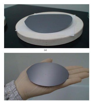
Figure 1. Photograph of silicon wafer after grinding and CMP. (a) Silicon wafer after grinding; (b) Silicon wafer after CMP with 3 hours.
上一篇: 单片炉的设计及在快速热处理中的应用
下一篇: 金属蚀刻残留物对蚀刻均匀性的影响