Scaling of gate lengths has led to signifificant improvement in semiconductor device performance. However, fabrication complexities have also increased and surface defects control becomes very critical for yield enhancement. In particular, chemical mechanical polishing (CMP) process is considered as one of the dirtiest processes to wafer surface contamination. And brush scrubber is the most effective method for post CMP in situ cleaning. Many literatures have reported brush scrubber mechanism and proposed particle removal effificiency based on remaining particles at post brush scrubber cleaning. However, concerns associated with brush to wafer surface contamination have not been addressed properly although real manufacturing has a lot of issues on that effect. This paper discuss cross contamination at brush scrubber process and emphasize that optimum cleaning should consider brush cross contamination in addition to brush particle removal effificiency.
Introduction
Chemical mechanical polishing (CMP) becomes an enabling technology for Fin Field-Effect Transistor (FinFET) device fabrication and process complexities are very much increased as compared to the planar device nodes [1–5]. In addition to its planarization function, defect reduction in the CMP process itself draws serious attention for device manufacturing. Major defects from CMP process are slurry abrasive particle, abraded fifilm, organic residue from polishing pad, particles from the tool, and micro scratches [6]. CMP tool has polisher module and in situ cleaning module which can drive defects on the wafers. Except for micro scratch, in situ cleaning is mainly responsible for particles removal before wafer dried out. Depending on the tool manufacturer, in situ cleaning module use different cleaning processes, such as megasonic and brush scrubber. Among various cleaning methods, brush scrubber cleaning is the most popular and effective method in CMP tool because of its single wafer processing, low cost of ownership (COO) and high cleaning performance by physical force. Most of the brushes used in CMP in situ cleaning are made of polyvinyl alcohol (PVA) material and composed of a lot of cylindrical nodules on the surface. Each cylindrical nodule has meshed structure, with lots of pores. Cleaning performance is determined by kinematics of brush module, brush design, mechanical properties of brush and chemicals flflowed in the brush [7–9]. For FinFET devices, post CMP defects can directly impact yield loss and critical killer defect size becomes very small with shrinking gate lengths. For example, W residue and organic residues can be root cause of M1 electrical short and open contacts [5,10]. Multiple studies and research works have been done to analyze brush cleaning performance with focus on particle adhesion and removal mechanism, tribology and contact mechanics, and cleaning chemicals [7,11– 12]. From these studies, the importance of hydrodynamic drag force and criteria for particle removal was highlighted. Recent study by Sun et al. [13] also outlined the effect of brush design and its mechanism for particle removal. However, all studies have investigated only particle removal aspects, and contamination from brush itself was not considered much, which can be direct source of organic residues. This paper shows strong evidence for particle contamination coming from brush to the wafer surface and results of experiments performed to understand the effects of brush rotation speed, brush gap and de-ionized wafer (DIW) flflow rate for brush generated particle contamination.
Experimental details
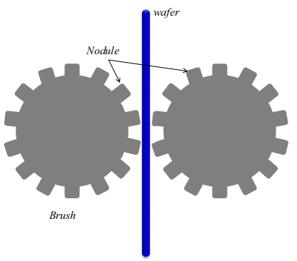
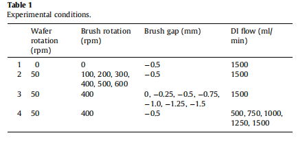
Reflflection-LK model CMP tool from Applied Materials Inc. was used for post CMP in situ cleaning experiment. Its post polishing cleaning module is composed of megasonic tank, 1st brush scrubber, 2nd brush scrubber, and isopropyl alcohol (IPA) dryer. The schematic of brush cleaning module is shown in the Fig. 1. Wafer is located vertically in the brush cleaning box and wafer as well as brushes is rotating for effective particle removal. It also has spray bars above brushes and either chemical or DIW flflows from spray bar and flflows through the brush core. In order to investigate particle cross contamination effect, 300 mm tetraethyl orthosilicate (TEOS) blanket wafers were used for this study. TEOS thickness was 3 kÅ for all experimental conditions. To focus on only brush effect, TEOS blanket wafers ran in the one brush module (processed with 1st brush scrubbing) only without polishing, and dried out. To explore slurry abrasive contamination, wafers ran with silica slurry CMP before experiment and brush lifetime less than 500 wafers was used for all these experiments. Table 1 gives summary of details for experimental conditions. Rotational speed, brush gap, and DIW flflow rate were set as variables for these experiments. We defifine brush gap as distance between wafer surface and brush nodule, which means smaller gap creates high pressure to the wafer. Post defect characterization was performed by SP3 tool from KLA Tencor Inc., which is commonly used tool for defect inspection in the semiconductor area. And inspection resolution is to detect defect size of 65 nm and above. Scanning electron microscopy (SEM) review was done afterwards to identify types of each defect. Since experiment performed without polishing, post defects are purely driven by cross contaminated particle from brush (here, it is defifined as CCP). Except DIW, no other chemical was flflowed in the brush clean module. And effects of brush gap and DIW flflow rate for CCP on the TEOS wafer were studied.
Results and discussions
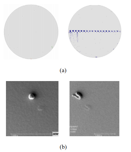
Fig. 2(a) shows wafer defect map and defect images from experimental condition 1 in Table 1. Before running wafer, pre-test wafer map is also provided in the same fifigure, and its total defects count (TDC) is less than 20, which can be ignored at post defect analysis. With brush contacting wafer with 0.5 mm brush gap for 30 s, strong brush nodule marks are observed as shown in Fig. 2(a) and adder defect count is over 3000. Defect was identifified with SEM and most defects were revealed as either silica particles

Fig. 1. Schematic of brush cleaner module in LK CMP tool.


Fig. 2. (a) Wafer defect map from SP3 inspection before and after brush contact and (b) defect images from (a) (after brush contact with experimental condition 1 at Table 1).
下一篇: 高效多晶硅太阳能电池的热氧化工艺