Photolithography is the engine that empowered semiconductor industry to reduce the minimum feature size of the components of a microchip from some 50 microns in the 1960s to below 14 nanometers today. Diffractive and refractive micro-optical components play a decisive role in modern photolithography systems, e.g. for laser line width narrowing, laser beam shaping (customized illumination), as phaseshift masks, for optical proximity correction, and for diffraction-based overlay. Wafer-based manufacturing of high-quality micro-optics and their importance for photolithography will be explained.
Photolithography Nowadays, we are used to have tens of Gigabytes of memory in our smart phones. Retail prices for flash memory are around one dollar per Gigabyte. In 1980, the first Gigabyte hard drive ever, the IBM 3380, weighed 250 kg and cost more than $ 80,000. Some ten years ago, a first Gigabyte SD flash memory card was introduced for a retail price of $ 500. The $ 500 will buy today’s leading edge SD cards with 512 GB, 500 times more for the same price. Semiconductor technology is moving forward with an incredible pace since more than fifty years. The driving force behind is “shrinkage”, also referred to as “die shrink”, i.e. the ability of semiconductor industry to reduce the minimum feature size of the components of a microchip from some 50 microns in the early 1960s to below 14 nanometers today. Die shrink allows manufacturing more chips on a wafer, reducing manufacturing costs, minimizing the power consumption and improving the performance in terms of speed, storage capacity and customer

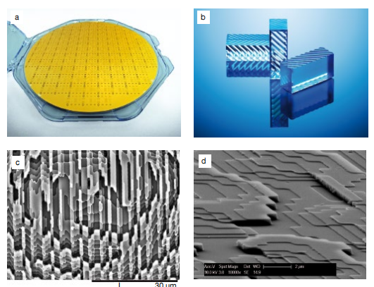
Fig. 1 8 inch wafer populated with diffractive and refractive micro-optical elements (gold mirror coating) (a); double-sided microlens arrays for beam twisting (b); and SEM images of 8-level diffractive optical elements (CGH) designed for laser beam shaping at 193 nm (c) and at 248 nm wavelength (d).
convenience. The key enabling technology behind shrinkage is photolithography. In a photolithography process, the layout of a microchip is copied onto a photosensitive layer on the wafer. In 1960s and 1970s, mask aligners in contact or proximity mode were the dominating photolithographic technology. They were replaced by scanners and projection steppers in the 1980s. In 1995, state-of-the-art projection lithography systems were operating at 248 nm wavelength providing a resolution of 250 nm (half-pitch). Nowadays, modern 193 nm steppers are able to print features below 40 nm (half-pitch, single exposure) – a fifth of the wavelength – and far below Abbe’s diffraction limit. Double patterning, multiple patterning, directed selfassembly (DSA) and other lithography enhancement techniques are used to achieve below 14 nm half-pitch today. A resolution enhancement from 250 nm resolution (single exposure) in 1995 to below 40 nm today was achieved by further improving the projection optics and by the introduction of immersion lithography, allowing a high numerical aperture of NA = 1.35. When lens optimization reached its very limits with surface qualities on the atomic scale, significant improvements could only be achieved by optimizing the mask illumination. Shaping the illumination light, also referred to as pupil shaping, allows the optical path from reticle to wafer to be optimized and has a major impact on aberrations and diffraction effects. Highly-efficient micro-optical components are perfectly suited for

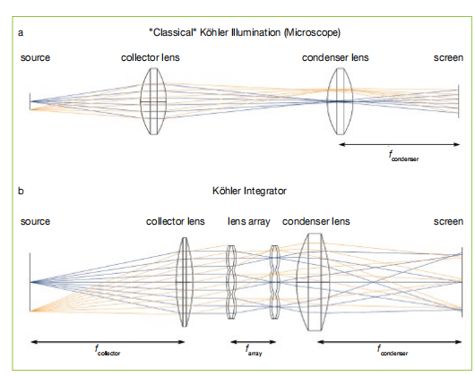
Fig. 2 Scheme of the classical Köhler illumination as proposed by August Köhler in 1893 for microscope illumination (a), lens-array-based Köhler integrator for flat-top illumination (b), scheme of two double-sided cylindrical microlens arrays as used for Köhler integrators (c); and photography of a mounted microlens-based Köhler integrator as used for mask aligner illumination systems (d).
上一篇: 高效多晶硅太阳能电池的热氧化工艺
下一篇: 晶圆级微光学工艺