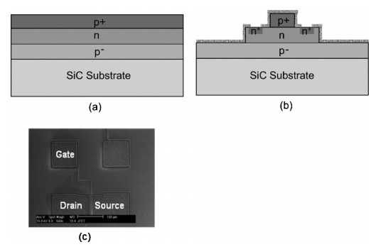
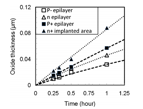
Silicon carbide has been considered as the most promising wide band gap semiconductor for high-temperature, high-voltage, and high-power electronics because of its excellent physical and electrical properties, including wide band gap, high electric fifield breakdown, and high thermal conductivity.1,2 A major advantage of SiC over other wide band semiconductors is its ability to form thermal oxide, which is a key component of metal-oxide-semiconductor fifield-effect-transistors MOSFET . Since a high quality gate oxide is pivotal for SiC MOSFETs, thermal oxidation of SiC has been extensively investigated3–6 and continues to be a very active research topic. In recent years, because of the carrier trapping issue in gate oxide of SiC MOSFET,7 there has been a growing interest in SiC lateral junction fifieldeffect transistors JFETs based integrated circuits IC for high-power and high-temperature sensing applications.2,8,9 The typical thicknesses of both p-type gate and n-type channel epitaxial layers of SiC lateral JFETs are less than 0.5 m. 2 Thermal oxidization of both p-type and n-type epitaxial SiC layers is an important process for isolating discrete SiC JFETs and passivating ICs. The thickness of thermal oxide directly affects the gate and channel thickness of SiC JFETs, which signifificantly affects the device characteristics. Therefore, it is important to predict the thickness of thermal oxide for both n-type and p-type layers on the wafer during thermal oxidation. In this short communication, we report the study of thermal oxidation kinetics of patterned n-type and p-type SiC layers on the same wafer for a short period less than 1 h . The doping concentration was found to signifificantly affect the kinetics of thermal oxidation. The substrates are 2 in. in diameter aluminum-doped 6H-SiC wafers purchased from Cree, Inc., 4600 Silicon Drive, Durham, NC 27703, USA. The wafers are 3.5° off axis and are silicon-terminated face. Three epitaxial layers were grown on the wafers as shown in Fig. 1 a . The thickness and doping concentration of the epitaxial layers were designed for lateral JFETs. The fifirst epilayer is a lightly aluminum-doped p− buffer layer with a nominal thickness of 7.0 m and a doping density of 1.2 1015 cm−3. The second epitaxial layer is a 0.33 m thick, nitrogen-doped n layer with a nominal doping density of 2.3 1017 cm−3for the channels of the JFETs. The top epitaxial layer is a heavily aluminum-doped p+ layer with a nominal thickness of 0.22 m and a doping density of 4.4 1019 cm−3 for the gates of the JFETs. The wafers were patterned as JFET structures using reactive ion etching RIE . 2 Figure 1 b shows a schematic cross section of a JFET structure and Fig. 1 c shows an optical micrograph of a fabricated SiC JFET. The source/drain contact areas were implanted with nitrogen ion at energies of 60, 40, and 20 KeV and doses of 1.1 1015, 7 1014, and 3.5 1014 cm−2, respectively, to achieve a box doping profifile.2 The simulated n+ concentration was about 2 1020 cm−3 for the above implant energies and doses.10 The implanted nitrogen was activated by annealing at 1200 °C for 30 min in a N2 atmosphere.2 The wafers were put into buffered HF solutions to remove all oxide before loading into a tube furnace for thermal oxidation experiments. Since the thermal oxidation rate is so slow at a temperature below 800 °C, the effect of wafer loading time on the oxidation kinetics can be neglected. A thin layer of oxide was grown thermally at 1150 °C in a wet ambient with a H2 flflow rate of 9 standard liters per minute SLPM and an O2 flflow rate of 6 SLPM. The thickness of the thermal oxide was measured by an optical method using a Nanospec AFT4000. The interfaces between the thermal oxide and SiC were in

FIG. 1. a Cross-sectional schematic of a 6H-SiC wafer with three epilayers, b cross-sectional schematic of the same wafer with patterned epilayers and nitrogen ion implanted regions, and c SEM micrograph of a fabricated JFET.

FIG. 2. Color online Oxide thickness as a function of time at 1150 °C. The symbols indicate measured results and the dashed lines indicate fifits by Eq
vestigated by high resolution transmission electron microscopy HR-TEM and x-ray energy dispersive spectroscopy XEDS on a FEI Tecnai F30 electron microscope., Hillsboro, Oregon 97124, USA. In a wet oxidation environment containing water vapor, thermodynamic calculations indicate that the primary reactions which occur for the oxidation of SiC are as follows:

In a dry oxidation environment containing only oxygen, reaction 1 governs the oxidation. The kinetics of dry thermal oxidation of SiC substrates has been studied by many researchers.3–5 The Deal–Grove model of thermal oxidation of silicon12 is still valid for thermal oxidation of SiC.3 In the case of wet thermal oxidation of SiC, the diffusion of CO and H2 from the interface between SiC and SiO2 to the wafer surface is included. There were only a few studies on wet thermal oxidation.6,13,14 The kinetics of thermal oxidation of SiC obeys the following equation:
上一篇: 微透镜压印光刻技术趋势
下一篇: 先进半导体技术现状及应用