1. Introduction
In 1994, about 20 years after the invention of the digital still camera and 10 years after first mobile phones appeared on the market, the first digital consumer camera, the “Apple Quick Take”, was introduced to the market. It took another 8 years until digital cameras were integrated into mobile phones. In the beginning, a mobile phone camera was just another gimmick with limited value for the mobile phone user. Memory was expensive, and the image quality was poor. Today, it is difficult to find a mobile phone without digital camera. Most mobile phones are now equipped with two cameras, a primary Mega-Pixel (MP) camera for photography and a secondary CIF or VGA camera for video calls. Far more than a billion mobile phone cameras were sold in 2007, and the numbers are still increasing rapidly.
2. Trends for Mobile Phone Cameras
It is difficult to predict long term developments in the field of mobile phone technology. Regarding mobile phone cameras, the situation is much easier, they will get better, they will get cheaper – but they remain to be an indispensable part of a mobile phone. Today, two main trends are observed: a) High resolution cameras, providing autofocus, optical zoom, mechanical shutter, stabilization and Xenon flash. Mobile phones equipped with high resolution cameras are in direct competition with digital still cameras. b) Wafer-Level Cameras, providing a high potential for cost-reduction in the low end camera market. The camera should be “reflowable”, i.e. it must survive standard SMT reflow soldering process at about 260°C. Both trends will certainly have a tremendous impact on the current optics and digital camera industry.
3. Wafer-Level Camera (WLC) T
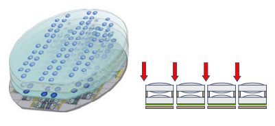
oday’s mobile phone cameras consist of some 10 to 20 different components like plastic or glass molded lenses, pupils, baffles, actuators, lens holders, barrel, filters and the image sensor. These components are manufactured and assembled by different sub-suppliers. The Wafer-Level Camera approach is rather simple: All components are manufactured on 8’’ wafer, the optowafers are mounted together with the CMOS wafer, and the wafer stack is diced into the individual camera modules. The complete mobile phone camera, including the optics, is manufactured and packaged on wafer-level using standard semiconductor technology.

Fig. 1. Wafer-Level Camera (WLC) concept. Optowafers and CMOS wafer are mounted together (left) and diced into individual camera modules (right).
Wafer-level imaging systems for mobile phones were already proposed more than 10 years ago [ 1 ]. First prototypes were shown about 5 years ago [2]. Since then, WLC technology was developed by research institutes like the Fraunhofer IOF and small companies like Heptagon, Anteryon and DOC/Tessera. It is worth to mention that most WLC research and development was carried out by the micro-optics experts, and not by manufacturers of mobile phone cameras. Recently, major mobile phone companies promoted WLCs as being the ultimate technology for next generation low-cost mobile phone cameras. Despite WLC technology is still not mature; all major camera suppliers are now investigating WLC solutions. The simplicity of the WLC concept often leads to the conclusion that CMOS manufacturers just have to use their highly developed semiconductor technology to manufacture the 8’’ opto-wafers.

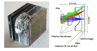
Fig.2. Wafer-Level Camera built in WALORI EU-IST Project [1]. Backside illumination through thinned CMOS image sensor and ball grid for bonding.
Compared to the 150 different process steps to manufacture a CMOS imager, the opto-wafers with some bulky lenses should be rather simple to do. In semiconductor industry “everything is possible” and further miniaturization is only a question of time. However, these assumptions are not valid for wafer-level optics:
Standard semiconductor technology is not suitable for the manufacturing of bi-convex aspherical lenses on 8’’ wafer level. • Well established materials from semiconductor industry can’t be used for wafer optics. • Most materials used for plastic optics do not survive reflow processes at 260°C. • In WLC the CMOS sensor is covered by the glass opto-wafers. Electric contact pads have to be place on the backside of the CMOS chip and Through Silicon Via (TSV) technology or backside thinning of the CMOS are required. • Fundamental physical laws limit a scaling down to ultra small cameras with high resolution. The WLC approach requires a close co-operation of optics and semiconductor industry with equipment suppliers. Novel technology has to be developed and existing production tools have to be modified.
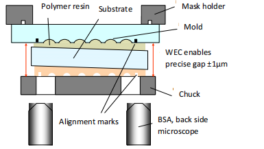
4. Microlens Imprint Lithography 8’’ wafer technology for refractive and diffractive microoptics was first implemented by SUSS MicroOptics in 1999. Standard manufacturing technology from semiconductor industry, like resist coating, lithography, reactive ion etching (RIE), deposition, sputtering, and lift-off were optimized to manufacture high-quality micro-optics in 8’’ Fused Silica, Silicon and Borofloat wafers. Unfortunately, the well-established 8’’ wafer technology is not suitable for WLC. Resist melting and RIE transfer do not allow manufacturing of microlenses with more than 100 µm lens sag. RIE speed of somemicrons per minute does not allow cost-efficient etching of bi-convex lenses on wafer level. The most promising technology is imprinting or UVembossing of polymer lens structures on glass wafers by soft PDMS stamps. First experiments to imprint microoptics on wafer level using a modified SUSS Mask Aligner MA6 have been carried out at the CSEM about 10 years agoCSEM’s microlens imprint technology has been transferred to Heptagon, also based in the Zurich area in Switzerland. Heptagon developed proprietary processes for reflowable micro-optics and is regarded as one of the pioneers in WLC technology. Recently Heptagon opened a WLC manufacturing facility in Singapore. Another pioneer in this field is the Fraunhofer IOF in Jena, Germany. They successfully developed replication and imprint technologies for low-cost wafer-level optics. Fully operable prototypes of ultra-flat cameras, endoscopes cameras and WLC systems have been presented. Microlens Imprint Lithography allows the manufacturing of lens arrays with a lateral accuracy of ± 1 µm on 8’’ wafer level.

Fig. 4. Microlens Imprint Lithography using a soft mold to imprint double-sided lens arrays onto opto-wafers.
上一篇: 微透镜阵列的制作及应用