Abstract Microlens arrays are the key component in the next generation of 3D imaging system, for it exhibits some good opti‑ cal properties such as extremely large feld of view angles, low aberration and distortion, high temporal resolution and infnite depth of feld. Although many fabrication methods or processes are proposed for manufacturing such precision component, however, those methods still need to be improved. In this review, those fabrication methods are categorizedinto direct and indirectmethod and compared in detail. Two main challenges in manufacturing microlens array are identifed: how to obtain amicrolens array with good uniformity in a large area and how to pro‑ duce the microlens array on a curved surface? In order to efectivelachievecontrol of the geometry of a microlens, indirect methods involving the use of 3D molds and replication technologies are suggesteFurther development of ultraprecision machining technology is needed to reduce the surface fuctuation by considering dynamiomachine tool in tool path planning. Finally, the challenges and opportunities of manufacturing microlens array in industry andresearch are discussed and several principle conclusions are drawn.
Keywords: Microlens array, Ultraprecision machining, 3D image system, MEMS
Introduction Natural compound eyes are extensively prominent in the biological optical systems of many diurnal insects or deep-water crustaceans, and such eyes consist of a mosaic of hexagonal ommatidia that work as tiny optical units [1–4]. Unlike single aperture eyes, natural compound eyes are characterized as having extremely large feld of view angles, low aberration and distortion, high temporal resolution and infnite depth of feld [3, 4]. However, the compound eye image system has intrinsic low resolution and sensitivity [4]. Te image resolution is subject to both the number and size of the ommatidia. If the image resolution of compound eyes increases to the same level as the human aperture eye, the radius of the overall lens would be at least 1 meter [5]. Although the image resolution and sensitivity of compound eyes are relatively low, microlens arrays, the artifcial counterpart of natural compound eyes, still havecrucial potential in a variety of applications in image systems, under the condition that high-resolution is not always required. For example, microlens array are more suitable in the extremely miniaturized imaging systems and 3D light feld cameras [6]. In addition, the high quality microlens arrays were applied in color imaging systems, 3D image acquisition systems and fngerprint identifcation systems [7–9]. Since the 1980s, the fabrication of microlens array is realized by diferent methods, such as Micro-electromechanical Systems (MEMS) based technologies [10–17] and ultraprecision machining technologies [18–20]. However, little work has been focused on the comparison of these method in terms of the surface fnish, form error and the efciency of production. One of the major challenge in the fabrication of the microlens array is the fabrication and assembly accuracy in a large area [19–21]. As the image resolution of a compound eye optical system is increased with the number of microlens and the radius of each microlens unit, enlarging the overall size of a microlens array can make up the defciency. However, to achieve the required uniformity in a large area is very diffcult [19]. Another challenge for microlens fabrication is producing microlens array on a fexible layer or a curved surface. Te curved artifcial compound eye is similar to the eye of the fruit fy Drosophila, which is more compatible and has a larger Field of View (FOV) [22]. Such curved compound eye imaging systems may have great potential in terrestrial aerial vehicles, visual reality systems, surveillance etc. Image detectors, such as conventional complementary metal-oxide-semiconductor (COMS) and charge-coupled device (CCD), are planar and not suitable for curved image systems. Recent developments [23] in fexible technologies enable the formation of microlens arrays on fexible substrates which are bent to a spherical surface. Similar to the problem in the fabrication of planar compound eye, the requirement of precise alignment of the photodetector and microlens is hard to achieve. In the light of the above, this paper aims to review the latest research on the progress of microlens array fabrication technologies. In Section 2, the operation principle of the compound eye is briefy introduced to provide background for the design of microlens array. In Section 3, the state-of-art technologies, including the direct and indirect methods for fabricating microlens array are reviewed and compared. Section 4 describes the applications of microlens array. Finally, the challenges and opportunities of manufacturing microlens arrays in industry and academic research are discussed and several principle conclusions are drawn in Section 5.
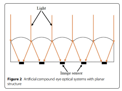
2 Principle of Compound Eyes In nature, compound eyes can be categorized into 2 types, e.g., apposition compound eyes and superposition compound eyes, as shown in Figure 1. In natural apposition compound eyes, the light through each ommatidia is received by only one photo receptor [1, 2]. In contrast, every photo receptor in the superposition compound eye is able to acquire light from several ommatidia. Terefore, superposition eyes are much more light-sensitive, and more suitable for deep-water crustaceans living in dim light. However, the main drawbacks of superposition eyes are the aberrations as the consequence of the combination of light from diferent ommatidia. Terefore, the artifcial compound eyes are mainly of the apposition form. As shown in Figure 1(a), in nature, the ommatidia of apposition compound eyes are arranged on a curved surface of radius Re and the receptors of diameter d are distributed on the focal points of the ommatidia. Te geometric size of each ommatidia is denoted by the pitch D and focal length

CMOS. Moreover, the fabrication process of microlens array on a plane is much simpler. For each unit of the microlens array, the geometric size is determined by the pitch (D), the height (h), the radius of curvature (Ru) and contact angle (θ), shown in Figure 3. Tese parameters can be measured through optical microscopy, scanning electron microscopy as well as contact proflometry. Te quality of the microlens often is denoted by the numerical aperture (NA), surface roughness and array uniformity.
上一篇: 晶圆级制造的热气动可调微透镜
下一篇: 微透镜压印光刻技术趋势