Abstract—This paper presents three coating methods of photoresist on large three-dimensional (3-D) topography surfaces. Two special methods, spray and electrodeposition (ED) are introduced and investigated for the fabrication of 3-D microstructures and RF-MEMS devices. Characteristics of each method as well as its advantage and disadvantages are outlined. A comparison is made to point out the most suitable coating method in terms of complexity, performance and type of application. The potential of these coating methods is demonstrated through several applications such as fabrication of multilevel micromachined structures and RF MEMS devices. [1031] Index Terms—Electrodeposition (ED), lithography for MEMS, patterning 3-D structures, photoresist coating, spray coating.
I. INTRODUCTION
T HE growing interest in the development of microelectromechanical systems (MEMS) and the increasing use of truly three-dimensional (3-D) microstructures requires new techniques and processes to fulfill the demand for further miniaturization and higher integration density. For several MEMS applications, pattern transfer onto silicon wafers with extensive topography requires a uniform photoresist layer over nonplanar surfaces. To date, three photoresist coating techniques have been introduced for the fabrication of MEMS devices. Spin coating is the most conventional coating method, which is applied to standard flat wafers. It is not always desirable and can only be used for some MEMS applications with certain modifications [1]. Alternatives such as electrodeposition and spray coating of photoresist should be considered. Electrodeposition of photoresist has been reported as an attractive method for 3-D stacks of chips [2], [3], but it requires a conductive layer. Recently, a new coating method, direct spray coating of photoresist, [4] has been introduced as another photoresist coating technique for microsystems. Although this technique is still in the early stages of exploration, it appears to be a promising technique for coating irregular surfaces as it presents some advantages over spin coating and electrodeposition of photoresist.

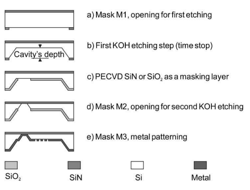
Fig. 1. Schematic drawing of the preparation of the wafers for coating experiments.
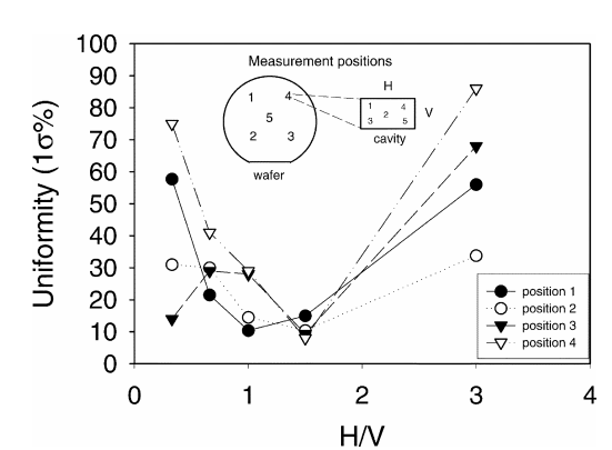
of the three coating methods is presented in order to identify the most suitable coating technique for a specific application.II. TEST MASK DESIGN AND WAFER PREPARATION The photoresist coating methods are used to transfer patterns in and across deep etched cavities. This highly nonplanar surface is often encountered in the fabrication of multilevel micromachined structures [5] and several RF-MEMS components. In order to evaluate all three coating methods, lithographic steps have been performed on micromachined silicon wafers. Deep anisotropically etched cavities of varying sizes and shapes have been anisotropically etched in KOH solution. The processing scheme used to evaluate the coating techniques is schematically illustrated in Fig. 1. Although cavities between and have been investigated [6], in this paper we focus on wafer with cavity’s depth close to . A set of test masks has been designed to study pattern transfer on these wafers. A first mask (M1) is needed to define the deep cavities and grooves. This mask consists of blocks of structures being repeated on different areas of the wafer. Each block contains several groups of rectangles or squares with different dimensions and with an H/V ratio varying between 0.6 and 5 (H and V indicate parallel and perpendicular orientation with respect to the flat of the wafer, see Fig. 2). Group A consists of several rectangles with dimension of 1 mm 3 mm and 2 mm 3 mm, which are placed both parallel and perpendicular. Group A’ has the same distribution of structures, but their dimensions are 2/3 of the ones in group A.

Fig. 2. Uniformity of photoresist spin coating versus the shape of cavities (cavity depth: 375 m).
上一篇: 先进半导体技术现状及应用