OVERVIEW: In the 0.1-µm age, it will be possible to build more than one billion transistors on a silicon chip welcoming in the “system-on-a-chip” era. This age will feature an even greater demand for high-performance and low-cost characteristics in LSIs, as well as Quick Turnaround Time (QTAT) from development to production. Device technologies and process technologies have progressed dramatically in recent years, with advanced technologies being driven not only by Dynamic Random Access Memory (DRAM) but also by logic products like microprocessors. Specifically, DRAM has been driving memory cell technologies and fine-processing technologies, and logic products have been driving high-performance transistor technologies and multilevel wiring technologies. Issues in the fabrication of memory cells are the selection of capacitor structure and its insulator film. On the other hand, the major issue in fine-processing technologies is dealing with inherent limits to miniaturization with excimer laser exposure equipment, and for feature sizes of 0.1 µm and smaller, shorter wavelengths or electron beam drawing will have to be selected. Achieving multilevel wiring technologies, moreover, will require the construction of a high-speed wiring system by decreasing wire resistance and decreasing inter-wire capacitance. In production technologies, innovative schemes for raising productivity will be needed to lower costs and deal with shorter product life cycles. Devising QTAT and high-yield technologies to shorten the time from development to production is an important issue here.

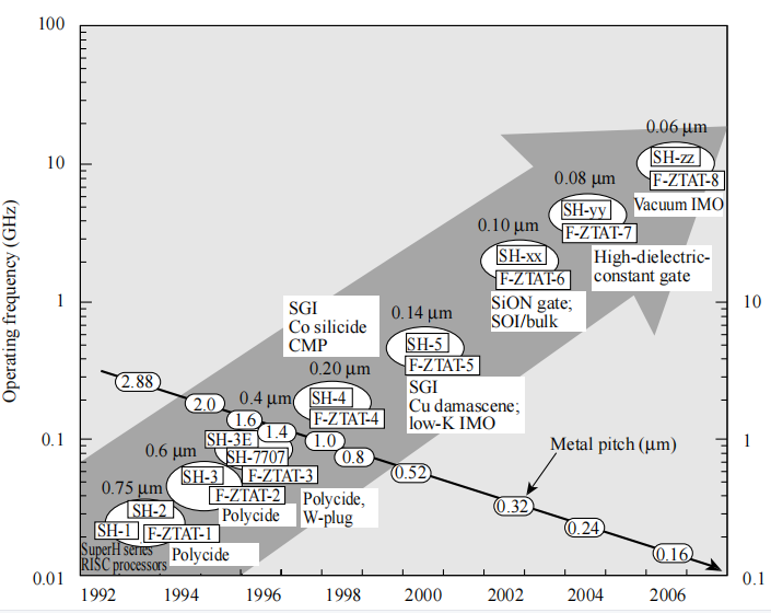
Fig. 1— Increase in RISC Performance Due to Miniaturization and Application of Advanced Processing Technologies. Hitachi, Ltd. has been raising the performance of system LSIs through the development of fineprocessing technologies and multilevel wiring technologies. The SuperH series of RISC processors are becoming faster and consuming less power over time.。
INTRODUCTION IN response to the 1994 publication of the “Technology Roadmap for Semiconductors” by the Semiconductor Industry Association (SIA) in the United States, the semiconductor industry around the world has been accelerating its development efforts to achieve the proposed targets early. Since 1997, however, the SIA Roadmap has been revised yearly, and its most recent version will have moved up the 0.1-µm (gate length in logic devices) age by two years (Fig. 2). With regard to manufacturing technologies, major factors behind this revision has been flattening of the process surface by the introduction of Chemical-Mechanical Polish (CMP), and further progress in fine-processing technologies through the application of excimer laser exposure equipment and resolution enhanced technology. It is also considered that miniaturization has been accelerating due to competition in producing low-cost Dynamic Random Access Memory (DRAM) and the achievement of higher speeds and lower power consumption in LSIs targeted for system-on-a-chip applications. This paper will focus on the 0.1-µm age due to arrive in 2001. We will describe high-performanceoriented device technologies and associated process technologies for shortening development Turnaround Time (TAT) and achieving high yields, all from theviewpoint of lowering cost in terms of production technology。
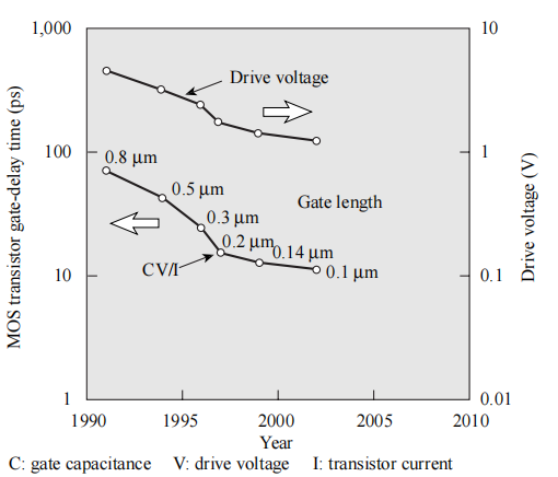
DEVICE TECHNOLOGIES High-performance Transistors Developing high-speed and low-power-consuming LSIs is essential to achieving a system-on-a-chip configuration. In particular, high-speed operation is necessary to perform complex and advanced information processing, and low power consumption is indispensable to achieving long operation time in portable equipment and decreasing dissipated heat in large-scale systems. To achieve high-speed operation, high-speed characteristics have been sought in Metal-Oxide Semiconductor (MOS) transistors, the basic devices of LSIs. In this regard, a critical factor in achieving high-speed performance is gate delay time in the transistor. The change in gate delay from one generation to the next is shown in Fig. 3. As can be seen, operation speed has been increasing every generation as drive voltage decreases. An important point here is that current can be made large even if drive voltage drops by shrinking the gate length and by making the gate insulator film thinner. However, as tunnel current increases for gate insulator film under 2 nm in the case of SiO2, studies have begun on。

Fig. 3— Trend in MOS Transistor Gate-delay Time and Drive Voltage. In conjunction with miniaturization of the gate length, gate delay time is shortened and drive voltage is lowered, thereby increasing LSI operating speed and reducing power consumption.