Semiconductor wafer bonding has increasingly become a technology of choice for materials integration in microelectronics, optoelectronics, and microelectromechanical systems. The present overview concentrates on some basic issues associated with wafer bonding such as the reactions at the bonding interface during hydrophobic and hydrophilic wafer bonding, as well as during ultrahigh vacuum bonding. Mechanisms of hydrogen-implantation induced layer splitting ~ ‘‘smart-cut’’ and ‘‘smarter-cut’’ approaches! are also considered. Finally, recent developments in the area of so-called ‘‘compliant universal substrates’’ based on twist wafer bonding are discussed.
I. INTRODUCTION ‘‘Wafer bonding’’ refers to the phenomenon that mirrorpolished, flflat, and clean wafers of almost any material, when brought into contact at room temperature, are locally attracted to each other by van der Waals forces and adhere or ‘‘bond’’ to each other. Historically, probably the fifirst report on the sticking of flflat glass plates can be found in a 1638 book by Galileo Galilei.1 Later on, this phenomenon was empirically known and partly used for optically polished pieces of materials and was fifirst scientififically investigated for polished pieces of quartz glass by Lord Rayleigh2 in 1936. In the sixties and seventies, this adherence phenomena was used for some isolated applications involving glass3 by van Bueren et al. or III–V compound wafers4 by Antypas and Edgecumbe. In the eighties, almost simultaneously researchers at Toshiba5 and IBM6 used this room temperature adhesion phenomenon followed by an appropriate heating step for silicon wafers in order to replace epitaxial growth of thick silicon wafers or to fabricate silicon-on-insulator ~ SOI! structures, respectively. Shortly afterwards, the bonding of structured silicon wafers was applied for the fabrication of micromachined pressure sensors and termed ‘‘silicon fusion bonding.’’7 In the meantime, wafer bonding has been applied to all kinds of materials combinations involving silicon or other materials.8 The wide availability of chemo-mechanical polishing in integrated circuit fabrication and of a variety of precision thinning approaches has led to a widespread and diverse use of wafer bonding. The application areas range from microelectronic devices based on SOI material to power devices, high voltage devices, optoelectronic devices based on III–V compounds,9–12 nonlinear optics devices,13 and microelectromechanical systems14 including pressure and acceleration sensors. Although wafer bonding can beapplied as a simple and elegant method to join equal or different materials, one of its main advantages appears to be the possibility to fabricate single-crystalline layers on top of substrates which may be either amorphous, poly-crystalline, or single crystalline with a large lattice mismatch and thus cannot be used for epitaxial growth of the desired singlecrystalline layers. In the present overview, we will concentrate on selected fundamental materials science issues associated with wafer bonding. Section II starts with processes occurring during room temperature silicon bonding including bonding under ultrahigh vacuum ~ UHV! conditions. Section III will deal with reactions which occur at the bonding interface during a subsequent heating step. In Sec. IV we will describe thinning procedures with special emphasis on hydrogen-implantation induced layer splitting ~ ‘‘smart-cut’’ and ‘‘smarter-cut’’! for silicon and other materials. Finally, in Sec. V we will highlight recent progress in the understanding of so-called ‘‘compliant universal substrates’’ based on twist wafer bonding. Since we will not cover all areas of wafer bonding and its applications, for a more extensive treatment of this fifield we refer the reader to recent conference proceedings,15–18 review articles,19–30 a special 1995 issue of the Philips Journal of Research31 and a book32 on this subject.
II. ROOM TEMPERATURE PROCESSES A. General remarks
Wafer bonding requires clean and mirror-polished surfaces which may be chemically conditioned before bonding. In the case of silicon wafer bonding, three principle kinds of surface conditioning are used: ~ i! hydrophilic surfaces which usually consist of an oxide layer ~ native oxide or thermally grown oxide! to which water molecules are attached via intermediate OH-groups, ~ ii! hydrophobic surfaces which consist of hydrogen saturated silicon surfaces obtained by an HF-dip removing any oxide layer, and ~ iii! clean silicon surfaces without adsorbates which may be realized only under

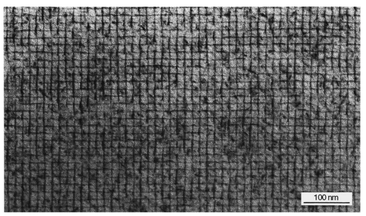
FIG. 1. Plan view TEM picture of screw dislocation network at interface of two ~ 100! silicon wafers bonded at room temperature under UHV conditions without any subsequent annealing treatment ~ Ref. 44!
上一篇: 电解水清洗用于半导体制造
下一篇: 磷扩散过程中的金属表面污染