ABSTRACT
In this work the etching of different Si-oxide (thermal oxide, TEOS as -deposited, TEOS annealed and PSG annealed). Sinitride (LPCVD and PECVD) and metal layers (A-Cu, Ti and TiN) in HF:H0 24.5:75.5, BHF:glycerol 2:1 and vapor HFis studied and compared. The vapor HF etching is done in a commercially available svstem for wafer cleaning. that waadapted according to custom specifications to enable stiction-free surface micro-machining. The etch rates as a function ofetching method, time and temperature (for HF vapor) are determined. Moreover, the influence of internal (temperature.nitrogen flow, wafer size) and external (sample pretreatment) parameters on the HF vapor etching process are analyzedbefore choosing the standard HF vapor etch technique used for comparing the etching behavior of the different films.
Auger depth profiles and infrared spectroscopy are used to explain the time varying etch rates of the metal films and thechanges in the Si-nitride films after HF vapor etching.
INTRODUCTION
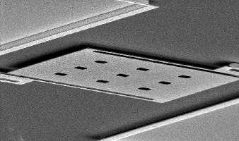
Surface micro-machined Micro Electro Mechanical Systems (MEMS) are often made by using poly-Si or poly-SiGe 1,2 as a structural layer and an oxide layer as the sacrificial layer. The sacrificial layer can then be etched with high selectivity towards the structural layer by the use of Hydrogen Fluoride (HF). The most widespread method of HF based etching is wet chemical etching in a mixture of HF and water or in a mixture of buffer HF with glycerol 3- 10. The latter is preferred when Aluminum structures are on the wafer as the addition of glycerol to BHF decreases the etch rate of metals. Drying of released wet etched structures however causes problems of stiction. Although solutions exist to overcome these problems, it is also possible to circumvent stiction by using an HF vapor release etch. Especially when the wafer temperature during the release is raised above 40 °C, a high yield can be obtained for the surface micro-machined structures 11 . An example of a surface micromachined poly-SiGe bolometer, fabricated by sacrificial etching of TEOS with HF vapor, is shown in figure 1.

Figure 1
2.EXPERIMENTAL PROCEDURE
2.1.Sample preparation
The blanket layers that were investigated in this work are four different Si-oxides, two different Si-nitrides and three metalbased films. The Si-oxide layers are 1200 nm wet thermal oxide grown at 975 °C, 1000 nm TEOS (tetraethoxysilan)deposited by a CVD process at 670 °, the same film annealed for 30 min. at 900 C and 1000 nm PSG (phosphosilicateglass) with 4.5 wt.% P grown at 550 C and annealed for 30 min at 750 °C. The 200 nm thick LPCVD nitride layer wasleposited at 770 °C, while the 1000 nm PECVD nitride was deposited at 400 C. The metal-based films are all deposited bysputter deposition. The titanium and titaniumnitride films are 200 nm thick and the Al - 0.5 wt% Cu film is 1000 nm thickAll these layers are commonly used in semiconductor and MEMS processing and can thus be present on the wafer duringthe sacrificial oxide etching.
2.2.Description etch procedure
For the wet chemical etching experiments two different solutions were used. The first solution consists of one part HF (49%) and one part DI water, resulting in a 24.5% HF solution in water or 14.2 mol. The second solution is made by mixingtwo parts of buffer HF (BHF) with one part glycerol (HOCH-HOCH-CH,OH). BHF itself consists of seven parts of NHF(40%) and one part HF (49%). The BHF/glycerol solution thus has lower concentration of HF, only 4 % or 9.4 mol1. Theetching will thus go slower for the BHFglycerol mixture compared to the HF/H0 mixture, but will also be more selectiveas will become clear from the measurements The experimental procedure used for the wet etching is as follows: afteretching a piece of a 200 mm wafer for a certain time in one of the solutions, the sample is put in a beaker with DI water fora few seconds after which it is rinsed in streaming DI water. After drying with a nitrogen gun, the film thickness is thenmeasured on at least five different places on the wafer. For the transparant films this is done by a spectrometer, for theconductive films this is done indirectly through a sheet resistance measurement if the ftm resistivity is assumed to heconstant, the sheet resistance is inversely proportional to the film thickness.
上一篇: 氢氟酸蚀刻后氧化碳化硅表面的化学性质
下一篇: 锑化铟和锑化镓晶体的生长和表征