Abstract
As predicted by the ITRS roadmap, semiconductor industry development dominated by shrinking transistor gate dimensions alone will not be able to overcome the performance and cost problems of future IC fabrication. Today 3D integration based on through silicon vias (TSV) is a wellaccepted approach to overcome the performance bottleneck and simultaneously shrink the form factor. Several full 3D process flows have been demonstrated, however there are still no microelectronic products based on 3D TSV technologies in the market - except CMOS image sensors. 3D chip stacking of memory and logic devices without TSVs is already widely introduced in the market. Applying TSV technology for memory on logic will increase the performance of these advanced products and simultaneously shrink the form factor. In addition to the enabling of further improvement of transistor integration densities, 3D integration is a key technology for integration of heterogeneous technologies. Miniaturized MEMS/IC products represent a typical example for such heterogeneous systems demanding for smart system integration rather than extremely high transistor integration densities. The European 3D technology platform that has been established within the EC funded e-CUBES project is focusing on the requirements coming from heterogeneous systems. The selected 3D integration technologies are optimized concerning the availability of devices (packaged dies, bare dies or wafers) and the requirements of performance and form factor. There are specific technology requirements for the integration of MEMS/NEMS devices which differ from 3D integrated ICs (3D-IC). While 3D-ICs typically show a need for high interconnect densities and conductivities, TSV technologies for the integration of MEMS to ICs may result in lower electrical performance but have to fulfill other requirements, e. g. mechanical stability issues. 3D integration of multiple MEMS/IC stacks was successfully demonstrated for the fabrication of miniaturized sensor systems (e-CUBES), as for automotive, health & fitness and aeronautic applications.
INTRODUCTION
Performance and productivity of microelectronics have increased continuously over more than four decades due to the enormous advances in lithography and device technology. However, today it has become questionable if the “traditional” device shrinking development alone will be able to overcome the performance and cost problems of future IC fabrication, e.g. caused by interconnect delay and latency issues. The ITRS roadmap predicts 3D integration as a key technology to solve this so-called “wiring crisis” [1]. The corresponding solution – 3D integrated circuits (3D-IC) - will most probably be based on through silicon via (TSV) technology.
World-wide several companies and research institutes have demonstrated 3D integration processes [2]. Even though there are still no commercial 3D-IC applications in the market, it has become apparent that there is a strong demand for such future applications including memories and processors. In addition to the enabling of further improvement of transistor integration densities (“More Moore”), 3D integration is a well-accepted approach for so-called “More than Moore” applications with their essential need for integration of heterogeneous technologies.
APPLICATION DEVELOPMENT
Which microelectronic products based on TSV technologies are at present actually in the market? CMOS image sensors (CIS) using a “via last” approach with via diameters of about 50 µm and similar silicon thicknesses have been already introduced in the market mainly driven by form factor. Actually today´s only commercial stacked TSV applications are not 3D-IC structures, but instead use backside vias. In Europe STMicroelectronics developed a 2M pixel mobilephone camera module VD6725 which is fabricated using TSV. The CMOS image sensor products are being fabricated in their Crolles facility [3]. Also other major CIS manufacturers, as Aptina, Samsung, Toshiba and ZyCube announced to use backside TSV processes for their future products.
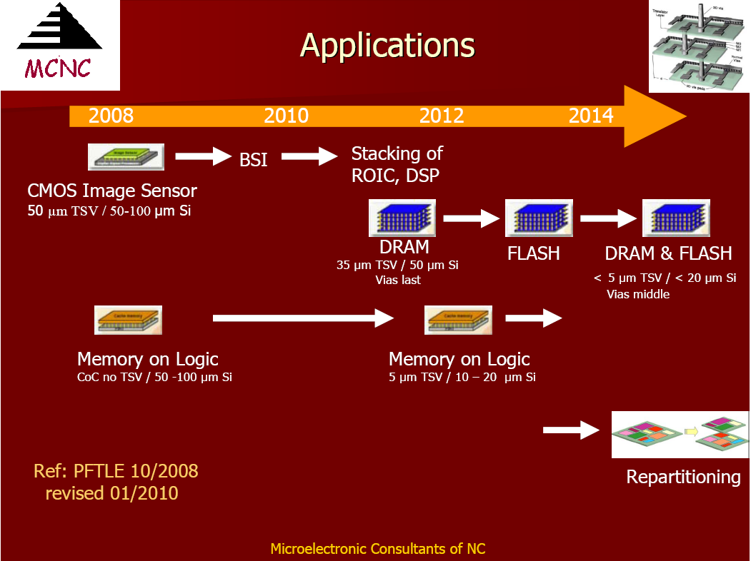
A strong demand for TSV technology is predicted in numerous publications and as well by many independent market reports (e.g. [4]). Thus clearly, future applications include memories and processors (see Fig. 1): 3D stacking of DRAM and NAND memories by applying TSV technology is in development and has been reported to be technically viable by e. g. Samsung, Elpida and Micron. Subsequently the stacking of Flash memories is expected to be introduced. The evolution of the corresponding fabrication technologies will result in combined DRAM/Flash products with TSV diameters of < 5 µm in ultrathin silicon of less than 20 µm. Chip-on-Chip (CoC) stacking of memory and logic devices without TSVs is already widely introduced in the market. Applying TSV technology for memory on logic will increase the performance of these advanced products and simultaneously shrink the form factor. Toshiba simulated a 16-core processor to quantify the impact of 3D integration (TSV) to CMOS technology (32nm node). In 2009 Samsung published the realization of an 8Gigabit DDR3 DRAM memory by 3D stacking using TSV technology [5]. The 3D architecture with one master and three slave chips enables I/O data rates of 1600 Mb/s. Elpida Memory has prototyped as well an 8Gigabit TSV DRAM and announced to schedule the fabrication of a 16 Gigabit product.

Fig 1
While in summary it shows up that the benefits of 3D TSV technology are widely accepted, the real initiation of commercial 3D-IC products is not expected before 2012. Apparently the high performance needs can not be met by current 3D TSV technologies with sufficient low production costs.
上一篇: 3D-TSV集成的材料和工艺研究进展
下一篇: 晶体硅结构的选择性湿蚀刻工艺优化