Abstract
In the aqueous processing of silicon wafers, drying of wafers must take place after each processing step. However, the drying processes currently used are not environmentally sound, i.e., great amounts of solvents and energy are consumed. To fulfifill environmental and economic requirements, a new wafer drying system based on concepts of clean technology was investigated. To reduce isopropyl alcohol (IPA) and energy consumption and to improve drying performance, a new dryer consisting of two separate chambers (IPA-chamber and drying-chamber) was developed. On-site operation with this new confifiguration was performed to compare its characteristics with those of other widely used dryers. It showed that IPA and energy consumption were smaller than those of the conventional dryers. Drying performance of the new dryer was also better than that of the conventional dryer. Consequently, the new dryer provides an environmentally friendly alternative to wafer drying.
Introduction
Semiconductors are electrical devices that perform information processing and display, power handling, and conversion between light energy and electrical energy. Semiconductors are used in computers, communication equipment, electrical control devices, robots, and numerous other electrical products. The semiconductor manufacturing industry is expanding to fulfifill desires to process information faster and more effificiently. A sizable industry expansion is also expected in this century [1].
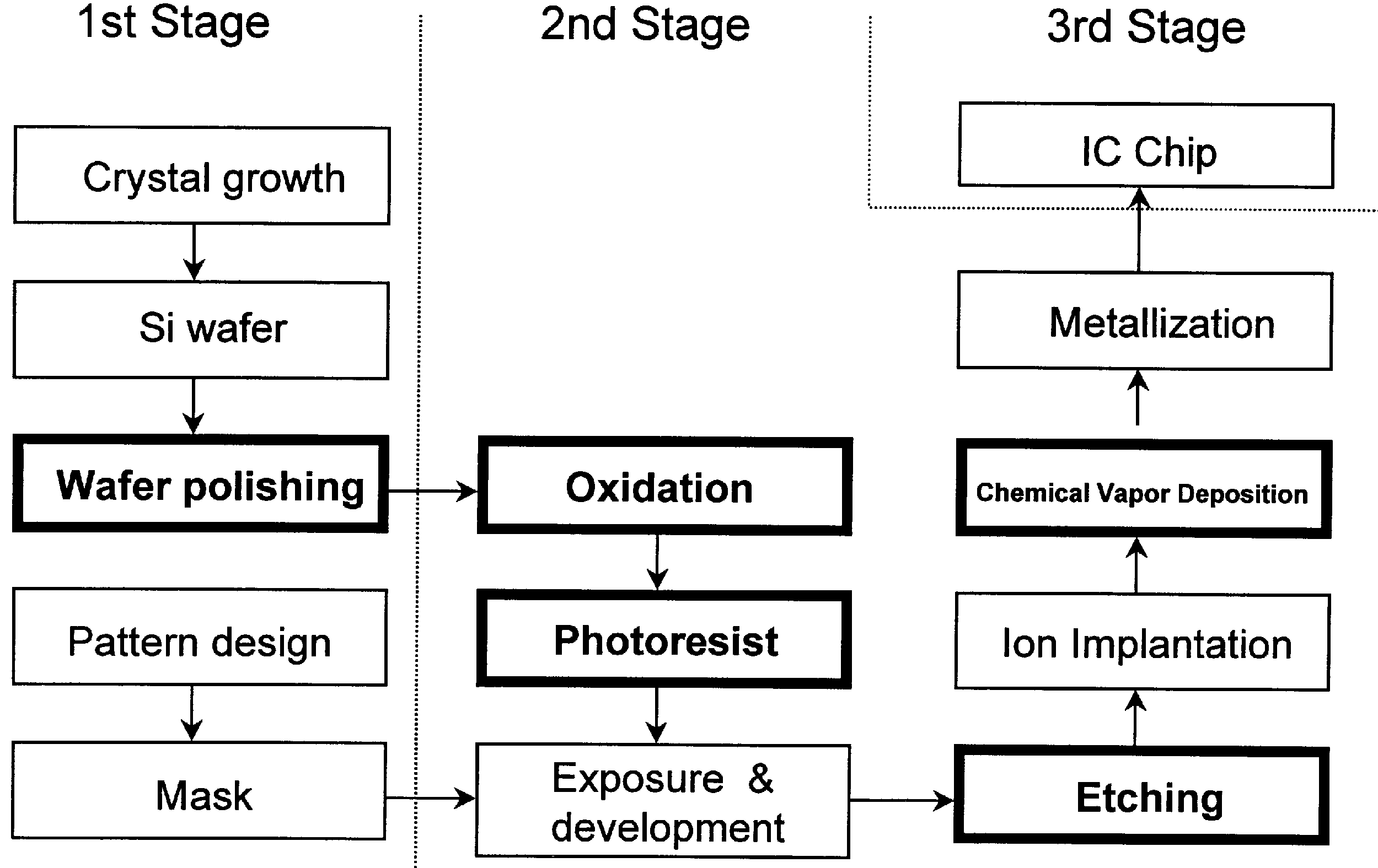
Semiconductor manufacturing is a complex operation involving several physico-chemical processes. The general process is shown in Fig. 1. As a fifirst step, a silicon wafer is produced by the crystal growth (1st stage). To give it semiconductor characteristics, the wafer processing (2nd stage) includes many steps such as oxidation, photoresist spreading, UV exposure, etching, ion implementation and chemical vapor deposition (CVD). Finally, the chip is produced through cutting and fabrication (3rd stage).

Fig 1
Every wafer-processing step is a potential source of contamination such as production of particles, inorganic and organic residues, which may lead to defect-formation and device failure. Numerous processes aimed at performing wafer cleaning have been developed [2,3]. Commonly used wet-cleaning techniques are still dominant because of their overall higher cleaning strength.
The last steps in every wet-cleaning process are rinsing and drying. Both are critical steps because clean surfaces become recontaminated easily if not processed properly. After wet-cleaning, rinsing is conducted with flflowing high purity deionized (DI) water. Finally, the drying step is required to prepare wafer surfaces for sub-sequent processing. Whereas the use of diluted chemicals and powerful ultrasonic has led to huge improvements in the wet-cleaning process, the fifinal drying still represents a performance bottleneck for cleaning equipment. Thus, it is recognized as a critical step of semiconductor manufacturing [4].
The most commonly practiced drying process is spin dry (SD). However, for today’s deep-submicron devices, it often fails due to the immense stress on the wafers. It has been suggested that this method recontaminates the wafer surface with particles and aerosols caused by mechanical motion of the dryer itself [5]. Another drying method is solvent vapor drying (VD), typically using isopropyl alcohol (IPA, 2-propanol) [6]. IPA strips the water from the wafer surface by the feature of the low surface tension of IPA. It is well known that VD using IPA provides several functional advantages over SD. But tremendous amounts of alcohol and energy are wasted, which raises costs of consumables and of environmental protection. Additionally, it causes safety concerns due to the high operating temperature [7].
Most conventional VD systems employ only one chamber where both IPA-vaporization and drying are carried out simultaneously. Since the operation of carrying wafers to and from the dryer is performed in the chamber where the liquid IPA is heated and vaporized, the chamber cannot be sealed [8]. The wet wafer surface can be exposed to oxygen so easily that this system creates a large quantity of “water-marks” (or “water-spots”) on the wafer surface [9]. The reaction between the wafers, water and oxygen is Si+H2O+O2→H2SiO3. Water-marks pose a signifificant challenge in the drying of silicon wafers because they can cause electrical failure due to locally thicker oxide and prevent proper adhesion of fifilms [10].
This conventional VD system loses much thermal energy as well as IPA vapor because it is not isolated from the surrounding environment. In addition, it is not free from the risk of fifire due to IPA vapor leakage. Therefore, this system is not considered to be an environmentally friendly process.
上一篇: 多晶硅锗的 MEMS 薄膜封装
下一篇: 沉积方法对颗粒去除效率的影响