Abstract
This paper presents an attractive poly-SiGe thin-fifilm packaging and MEM (microelectromechanical) platform technology for the generic integration of various packaged MEM devices above standard CMOS. Hermetic packages with sizes up to 1 mm2 and different sealed-in pressures (∼100 kPa and ∼2 kPa) are demonstrated. The use of a porous cover on top of the release holes avoids deposition inside the cavity during sealing, but leads to a sealed-in pressure of approximately 100 kPa, i.e. atmospheric pressure. Vacuum (∼2 kPa) sealing has been achieved by direct deposition of a sealing material on the SiGe capping layer. Packaged functional accelerometers sealed at around 100 kPa have an equivalent performance in measuring accelerations of about 1 g compared to a piezoelectric commercial reference device. Vacuum-sealed beam resonators survive a 1000 h 85◦C/85%RH highly accelerated storage test and 1000 thermal cycles between −40 ◦C and 150 ◦C.
INTRODUCTION
THE USE of above-CMOS microelectromechanical systems (MEMS) technology enables the integration of multifunctional devices or arrays on a single chip with increased performance and reduced size. In the past years, several CMOSintegrated MEM devices have been fabricated using IMEC’s poly-SiGe MEMS-last technology [1]–[3]. Packaging was done by chip capping or by placing a naked die in a fifirst-level package. MEM devices often need a hermetic and/or vacuum package, which is preferably processed on the wafer level, before dicing. To date, a variety of wafer-level packaging technologies have been developed as comprehensively reviewed in [4]. Chip capping by wafer bonding techniques is often used for MEMS packaging, yet thin-fifilm packaging allows for a fully integrated process with a higher device density. Epi-Si [5], [6], poly-Si [7], Si-nitride [8]–[14], Si-oxide [15], [16], alumina [13], [14], SiC [17], [18], and plated Ni [19] membranes have already been used for thin-fifilm packaging, but a generic above-IC poly-SiGe thin-fifilm packaging process is still missing.
In this study, using a new thin-fifilm capping process, polySiGe accelerometers and resonators were fabricated together with their poly-SiGe-based package. The whole process flflow is run at temperatures below 455 ◦C. Depending on the sealing method, sealed-in pressures of ∼100 kPa or ∼2 kPa were obtained. Hermeticity was proven in vacuum, air, and N2 atmosphere and, for the ∼2 kPa sealed packages, also during accelerated testing. A modifified version of this process has been used to hermetically package silicon-on-insulator (SOI) resonators at pressures lower than 10 Pa .
An example of a clamped-clamped (c-c) beam resonator with a 10 µm thick poly-SiGe cap before sealing of the release holes is shown in Fig. 1. The top metal on the substrate is made of AlCu, mimicking the top metal of a CMOS process. The MEMS structural layer is 4 µm thick. There are 3 µm gaps below and above the structural layer, which are formed by removing the sacrifificial oxide layers through the release holes. Later (not shown in Fig. 1), an AlCu sealing layer will be deposited on the cap.

Fig 1
In Section II, the detailed fabrication process flflow of the poly-SiGe MEMS and its thin-fifilm package is described. The evaluation and discussion of the 100-kPa sealed packages as well as the demonstration of the functional packaged accelerometers are shown in Section III-A. In Section III-B, the characterization and the long-term accelerated life testing of the vacuum-sealed beam resonators are shown. Section IV contains an outgassing study for blanket fifilms. Next, the results are compared with other thin-fifilm packaging technologies in Section V. Finally, conclusions are given in Section VI.
PROCESSING
Above-IC Poly-SiGe MEM Devices
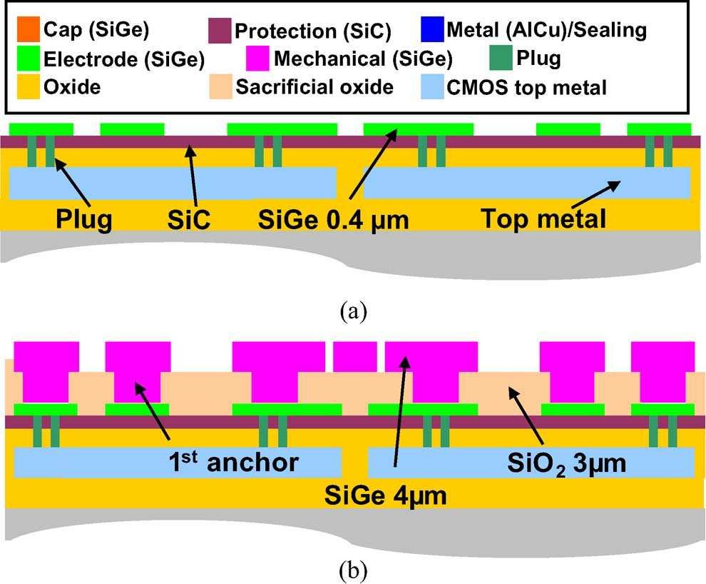
Fig. 2 shows the schematic process flflow of the MEM device before the integration of the thin-fifilm package. Poly-SiGe electrodes [Fig. 2(a)] and mechanical structures [Fig. 2(b)] are fabricated above a planarized standard back-end-fifinished CMOS wafer, as described in [1]–[3].

Fig 2
In this work, accelerometers and resonant beam structures are defifined on top of a simple AlCu interconnection that mimics the top metal of a CMOS back-end stack (Fig. 3). The AlCu interconnections and SiO2 insulating layers are protected by a SiC layer from HF vapor which is used during release process. SiGe electrodes of 0.4 µm thickness and deposited by thermal chemical vapor deposition (TCVD) at 0.6 kPa are formed on top of vias, which are fifilled with SiGe or W. After patterning the electrode structures, the wafer surface is planarized by the deposition of a SiO2 layer and chemical mechanical polishing (CMP) with stop on the electrodes.
下一篇: 晶圆干燥工艺中清洁技术的发展