Abstract
Embedded SiGe is applied in CMOS at recent technology nodes to improve device performance and enable scaling. The position of the SiGe surface with respect to the channel is found to have significant impact on the pFET threshold voltage and also on device variability. Therefore the recess etch and deposition of the embedded SiGe has to be very well controlled. We show the sensitivity of the device to the fill process and describe the feed forward and feedback techniques used to optimize the control of epitaxy.
INTRODUCTION
At the most recent CMOS technology nodes to enter manufacturing, there is an increasing need to add technology elements to boost device performance, since the traditional scaling of gate length and thickness no longer provide the required gains of higher saturation current (Id,sat) at lower drain voltage (Vd). Here we refer to techniques such as stress engineering, laser anneal, high k dielectrics and metal gates. In this paper we discuss the application of embedded SiGe (eSiGe), a form of stress engineering and a very powerful way to increase pFET device performance [1,2]. We show that the recess reactive ion etching (RIE) and epitaxial layer thickness should be very well controlled to avoid a significant increase of the variability of the pFET threshold voltage (Vth).
As mentioned, stress engineering is one of the most important tools at our disposal to boost device performance at the current nodes. The technology described here is the 45 nm half-pitch silicon-on-insulator (SOI) CMOS. In addition to the eSiGe, the subject technology employs several other strain-enhancement elements aimed at achieving optimal FET performance, i.e. dual stress liner, which will not be discussed here [1].
TECHNOLOGY DESCRIPTION
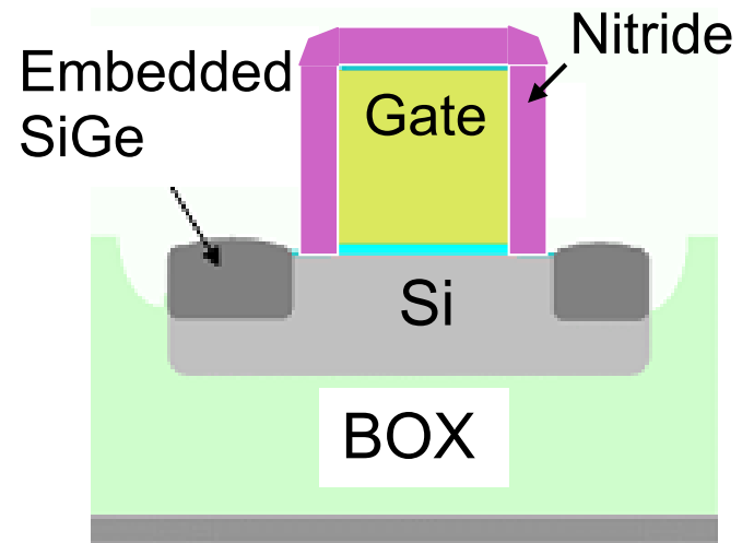
In SOI technology the active silicon rests on a so-called buried oxide layer (BOX), which in turn sits on a silicon wafer. The SiGe is deposited after definition of the gate. First the surface is covered with a nitride layer, which is opened over the source/drain region of the pFET device. Subsequently we etch the silicon in the opened area to a specified depth and then selectively deposit SiGe. We use a conventional technique using Silane, in which SiGe does not grow on the nitride [3,4].
The nitride also acts as a spacer defining the proximity of the SiGe to the channel (Fig. 1). After SiGe epitaxy the nitride is removed selectively and processing continues as conventionally, which in the present case means a gatesidewall spacer and a sequence of n and p halo and extension implants. A cross section of the device after SiGe deposition, but before removal of the nitride spacer, is shown in fig. 2.

Fig 1
The main reason the pFET is very sensitive to SiGe fill is the impact of the SiGe surface on the ion implants determining device threshold voltage, the extension and halo implant. The halo implant, an arsenic implant applied after definition of the polysilicon gate which counteracts the short channel effect[5], is particularly affected by the surface. To achieve the maximum benefit from the SiGe induced stress the eSiGe is deposited very close to the channel [6,7], which means the implant will take place largely through the SiGe surface. This in turn implies that even small variations of the SiGe deposited thickness will have considerable effect on the dopant profile and thus on device properties. The schematic of figure 3 illustrates the sensitivity of the profiles to the SiGe surface. To circumvent this issue it has also been proposed to move the SiGe deposition step to a later stage of processing, the so-called eSiGe S/D last [8].
上一篇: 沉积方法对颗粒去除效率的影响
下一篇: 退火条件对电镀Cu-TSV微观结构的影响