Abstract
In this paper, the effect of annealing condition on the microstructural and mechanical behavior of copper through-silicon via (Cu-TSV) is studied. The hardness of Cu-TSV scaled with the Hall–Petch relation, with the average hardness values of 1.9 GPa, 2.2 GPa and 2.3–2.8 GPa, respectively for the annealed, room temperature (RT) aged and the as-deposited samples. The increase in hardness toward the top of the as-deposited sample is related to the decrease in grain size. The annealed and the as-deposited samples showed a constant elastic modulus (E-modulus) value across the length of Cu-TSV of 140 GPa and 125 GPa respectively, while the RT aged sample showed a degradation in E-modulus from the bottom of the TSV (140 GPa) to the top (110 GPa). These differences in E-modulus values and trends under the different test conditions were found to be unrelated with the crystallographic texture of the samples, but could be related to the presence of residual stresses. No correlation is found between the hardness and E-modulus data. This is attributed to the coupling and competitive effects of grain size and residual stresses, with the grain size effect having a dominant inflfluence on hardness, while the presence of residual stresses dominated the E-modulus result.
Introduction
The need for increased portability and functionality in consumer electronic devices has pushed the microelectronics industry to develop smarter interconnection techniques. This has resulted in the birth of three-dimensional stacking of chips, which is achieved by the use of through-silicon via (TSV). This is an interconnection method in which holes are drilled through active chips, after which they are fifilled with an interconnect material. Different tiers of chips are then stacked on each other by Cu–Cu bonding or by the use of micro-bumps [21]. The TSV technique results in high chip performance since it yields high interconnect density and decreases signal delays and capacitance as it reduces the length of the electrical path. Even though there are many interconnect materials that are currently used for the fifilling of TSVs, copper (Cu-TSV) is the most preferred. This is because of its high electrical conductivity, relatively well-known deposition process and high resistance to electromigration which results in a large current-carrying capacity [1]. While there are a lot of documented research studies regarding the use of copper as an interconnect material in Back-End-Of-Line (BEOL), very little research studies exist for Cu-TSVs. Therefore, since Cu-TSV is the future for the interconnection of stacked chips, there is a need to understand and characterize its mechanical and thermo-mechanical behaviors. All studies done so far on mechanical behavior of Cu-TSV have been focused on their mechanical properties in the as-deposited state [2–4, 11]. Therefore, in this paper the impact of annealing conditions on the microstructural and mechanical behavior of Cu-TSV is studied.
Sample preparation
Vias of 5 μm diameter and 23 μm depth were prepared by deep reactive ion etching of 200 mm silicon wafers. First, a 100 nm thick silicon oxide is conformally deposited by chemical vapor deposition. A barrier layer of tantalum (80 nm), followed by a seed layer of copper (300 nm), was respectively deposited by sputtering on top of each other using Applied Endura CuBS (Cu Barrier/Seed) PVD (physical vapor deposition) with the self-ionized plasma (SIP) EnCoRe II process.
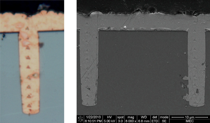
This is then followed by electrochemical fifilling of the via with copper. A large amount of Cu remains on the wafer top surface which is called the overburden. Details on the deposition chemistry and electroplating process have been reported in [5]. The samples were ground and polished to reveal the cross-section of the Cu-TSV and to obtain a flflat planar surface. Afterward nano-indentation (see figure 1), focused ion beam (FIB) and electron back scattered diffraction (EBSD) analysis were performed.

FIG 1
Experimental tests and procedure
In this study three annealing conditions (table 1) were studied by nano-indentation, EBSD and FIB analysis. The test conditions were chosen to mimic the effect of processing on the evolution of the mechanical and microstructural behavior of Cu-TSV from its initial state after electroplating (as-deposited state) to its fifinal state after the Cu–Cu bonding process. The bonding process is done at 300 ◦C for 15 min, prior to which the Cu-TSV has undergone a heat treatment at 420 ◦C for 20 min, which is called the sintering step. In between the initial and fifinal states, the effect of room temperature (RT) aging on CuTSV was also assessed. The RT aging was done for a 6 month period.
上一篇: SiGe的蚀刻和沉积控制
下一篇: 铜电解沉积技术