ABSTRACT
Through-Silicon-Vias (TSVs) continue to stand out as the most promising technology for electrical interconnections in the microelectronics industry. As package size continues to decrease, TSVs offer an elegant and robust solution for vertical interconnects. They facilitate 3D die stacking while minimizing or even eliminating area consuming planar packaging, allowing for direct signal and power paths through the substrate itself. TSVs can also be fabricated from different materials to desired dimensions to handle the required current level. Plated copper is emerging as the material of choice for TSVs. In this work, electroplated copper TSVs were fabricated successfully and evaluated using cutting and polishing techniques in preparation for image capture. The detailed fabrication process and analysis of the resulting TSVs are presented in this work.
INTRODUCTION AND BACKGROUND
With the ever decreasing package size of microelectronics, there is a natural tendency towards a more robust interconnect technology with minimum feature size and area foot print. TSVs are emerging as the interconnect technology to fit this demand. TSVs have been commercially utilized in many different devices, including cameras [1] video cameras [2], and DRAM [3]. Package sizes and power consumption can be significantly reduced with TSV technology due to shorter path lengths. Different approaches exist for developing TSVs. The via etching method was our first consideration in creating a robust TSV process. Etched vias can be fabricated using wet or dry etching processes. Wet chemical etching is crystal structure specific, potentially making wet etching very sensitive to process variations. Wet etching also uses caustic chemicals, making it less desireable. Two methods of dry etching were considered, Laser Ablation (LA) and Deep Reactive Ion Etching (DRIE). Laser ablation requires non-semiconductor specific equipment including a high power laser, high precision positioning stages, and custom control software. LA vias have been attempted by researchers with certain difficulties observed [4,5]. Additionally, LA may produce overly sloped sidewalls with significant roughness. Seed layer deposition on such an unpredictable surface can lead to voids and partial filling of the via during the plating process. Therefore dry chemical etching is the preferred etch method for creating consistent high aspect ratio geometries. DRIE is a plasma etching process that uses conventional semiconductor equipment and processes. This allows TSV processing to be easily integrated into existing silicon microfabrication process lines.
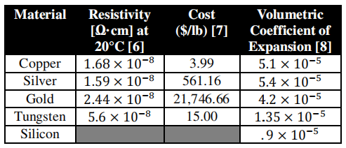
Our second consideration was which material to use to fill the vias. There are many conductors that can be used for this purpose. Cost, resistivity, and process compatibility were the main deciding factors. In addition, the volumetric coefficient of expansion, β, of the materials should be taken into long-term consideration. Over time, the expansion and contraction of the plated metal may have detrimental effects on the lifetime of the device. Finding a material to fill the vias that best matches the volumetric coefficient of expansion of silicon may produce a higher yield for long-term, extreme temperature, and high current density devices. For the context of this paper, the low resistivity and cost of copper, as well as its use in commercial devices, were the deciding factors in pursuing copper as the fill material. A variety of possible plating materials are listed and compared in Table 1.
Table 1: Resistivity, Cost, and Volumetric Coefficients for TSV fill candidates

TSV DESIGN AND FABRICATION PROCESS
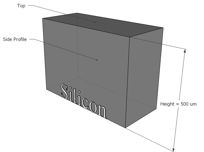
For the prototype device developed here, the diameters ofthe TSVs were 100um and the depths were 200um deep. Theywere spaced 30um edge-to-edge in a straight line. Since theprocess is orientation independent an arbitrary Si waferorientation (100) was chosen. A 500um wafer thicknessprovided a robust substrate for processing. Figure 1 is a 3Drepresentation of the bare Silicon wafer. Substrate wafers werecleaned using a standard RCA process to remove any organic.oxide, and metal contaminants [9]. A spin-rinse-dry was thefinal step prior to photolithography.

Fig 1
A positive photoresist, AZ P4620, was utilized for thephotolithography process. In DRIE, this photoresist hasapproximately a 70:1 selectivity with Si. It was chosen for itsmaximum spin on thickness of up to 24um. This yields asufficient thickness to achieve an etch depth up to the full waferthickness. The photolithography process was performed in 5 steps:
1.120°C dehydration bake for 30 minutes to vaporizemoisture, remove organics, and heat the wafer.2. Primer application (for this research HMDS). Primeradheres well to the naturally oxidizing silicon surface.3.Spin-on of photoresist (Figure 2), soft baked at 110°Cfor 2.5 minutes.4. Pattern exposure on a Karl Suss MA/BA6 contactmask aligner.5. Photoresist Development (Figure 3) in a 2:1 mixtureof DI water (200mL) and AZ 400K (100mL) developer. Waferinspected for under/over developing
上一篇: 铜电解沉积技术
下一篇: IPA溶液的界面和电动特性