Abstract:
A big yield drop has been observed during the automatic inspection (AOI) after the saw stage. A step by step AOI inspection check and defect review is made to see which step made a big yield drop and which kind of defect contributed most to the yield drop. Scanning electron microscope (SEM) and energy dispersive spectrometer (EDS) analysis showed the shape and chemical element of the particle. From the EDS result, particles can be separated into two categories. One was the inorganic related materials, mainly including silicon (Si) element, which came from the saw stage. A design of experiment (DOE) is used to find some reasonable saw relative parameter and optimize it in order to remove the particle from the saw stage. But the quantity of this kind of particle was small. Yield was only improved by less than 5%. Our main effort was to remove another
kind of particle which was organic related materials, mainly including carbon (C) and oxygen (O) element. This kind of particle was from tape residue. In order to remove the tape residual, one step was added before the saw stage. Almost all of the tape residual was removed. Finally, the final yield was improved by more than 15%.
Introduction
AOI equipment has been used in semiconductor manufacturing processes for many years, especially on die sale or wafersale parts, for quality control and improving manufacturingyieldlll. Yield improvement is an important job for us, as it canincrease profit to our company. In this paper, most of the yielddrop at the AOI step is contributed by particles. Particles inelectronic packaging assembly have always been a very challenging job to remove2-7]. Some particles will directly resultin quality failure and the other might induce reliability issuesIt is very significant to find the root cause of particles, identifit, describe how it happened and then remove it. Meanwhileparticles could be from a variety ofsources, such as direct material, indirect material, the environment, equipment, and evenhuman[8l. In the past, lots of research has investigated defectformation9-15]. In this paper, a novel method was thought outto remove almost all of these particles so that the final yield isimproved by more than 15%. If the output for this product isabout 10 wafers per day, the total dice on one wafer is 2500, andthe price is about 5 dollars per die, then after this work our com-pany gets an additional 2500x 15% x 10 x 365 x 5 =6 843 750dollars per year. It is a big yield improvement.This paper will provide a detailed review of the procedurefor removing particles.
Particle trace
As there was only one AOI check after the saw stage, therefore which step produced more particles was unknown. So 10wafers were used for this experiment. An AOl check step wasadded after every step and we recorded it to find which stepcontributed on the yield drop. See Fig. 1 about the process flowfor this part.
In order to find the source ofparticles, two AOI check steps were added after incoming and probe steps respectively. Afterthe incoming step, a clean function was used in the saw machine and then an AOI was run on all of the wafers. The average yield was 85.7%. Review results showed that almost allthe defects were FAB issues, including surface scratch, missingmetal, pad corrosion and little particle. Then all 10 wafers wereprobed and operated with the AOI inspection step. The averageyield was 83.4%. The review result showed that the additionaldefect was a particle, which should come from the probe ma-chine. The wafer was probed at the clean room, which was 10Kclass, and there should be some particles in the environmentSo the yield drop was normal and could be removed by thesaw clean step. The saw clean function was used to clean all the wafers, then the AO was performed again. The yield cameback to 85% level. Then all the wafers were sawn and the AOIwas checked again. The yield had dropped by about 15%. Nowthe yield was at the 70% level. The saw step contained a cleanstep, meaning the 15% yield drop could not be removed by theclean function. After reviewing all ofthe defects we found thatalmost all the additional defects were particles. From this ex-periment, we knew that the big yield drop was caused by thesaw step and the yield drop reason was particles.
Particle analysis
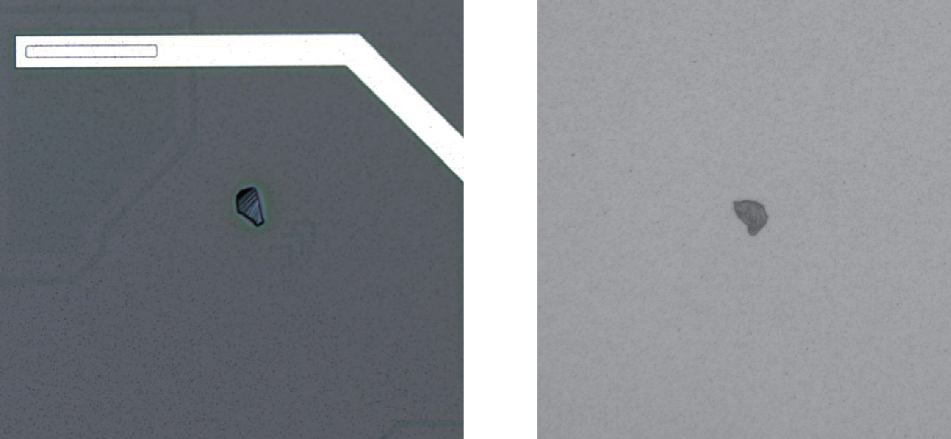
All these particles were observed under a microscopewhich magnified images 50 times. See Fig. 2. From the shapewe could see that these two particles should be different typesas one is transparent while the other is opaque. We need to learnthe element for both types of particles then find a method to remove them.

Fig 2
Some different types of particles were selected as the sam-ple and sent them to the lab to do SEM and EDS analysis to check the chemistry element. See Fig. 3 and Fig. 4. EDS results showed that there are two kinds of particles. Fig. 3 showsthe inorganic related materials, mainly including a Si elementThe defect dimension was about 40 um. Fig. 4 shows organicrelated materials, mainly including a C and O element. The dimension of this defect was about 8 um. Both of them camefrom the saw stage. For the Si particle, it was a silicon residualduring the saw process, which was too big to be removed bythe clean system. In order to resolve this kind of particle, thesaw or clean parameter should be optimized. For the C and Oparticle, it came from tape residual because only the tape mate-rial had organic related materials. As the tape was very stickybefore the UV stage, if tape residual adhered to the surface ofthe die, it was hard to remove.
上一篇: 动态化学镀铜沉积
下一篇: 高温IPA过滤器颗粒去除效率评价