1. Introduction
Recently, the necessity for global environmental conservation and the reduced use of electrical energy and decrease of CO2 have led to the development of energy-saving systems. Electrochromic devices (ECDs) and especially “Smart windows” as energy efficiency-related have recently attracted considerable attention because of their low switching voltage, the ability to display various colors, high reflective contrast ratio, large viewing angle, memory effect and long-term functioning. The properties of transition metal oxides, serving as functional layers in ECD are mainly determined by their specific band structure and electron distribution. They possess d-electrons, which create d-band partially overlapping s-band. The d-band provokes the interesting chemical, physical and optical properties of transition metal oxides. Electrochromism is defined as effect of color change caused by applied voltage and has been found in several different metal oxides, the metals belonging to transition series. This experimental fact suggests close relation between electrochromic properties and electronic structure of the functional material.
2. Experimental
Using our experiences in WO3 and MoO3 film depositions, mixed films on their basis were deposited. The precursors are the corresponding hexacarbonyls. The hexacarbonyl precursors (W(CO)6, Mo(CO)6 were mixed in a ratio Mo(CO)6:W(CO)6=1:4. The deposition proceeded in argon-oxygen rich ambient at atmospheric pressure (APCVD process) in a horizontal cold walls CVD reactor. The precursor powder placed in a sublimator immersed in silicon oil bath has been heated at temperature of 90o C and has been controlled with an accuracy of ±1o C. This sublimator temperature provides a sufficient vapor pressure of the hexacarbonyls. The gas lines (“Galtek” type Teflon) were heated up to the sublimator temperature in order to assure successful transport of the vapors to CVD reactor. Argon (99.995%) flow carries the precursor vapors to the reactor. The selected flow rate of Ar through the sublimator assures a constant amount of the precursors vapor. Through a separate line, oxygen (99.95%) enters the reactor. In the present study the ratio of flow rates of Ar/O2 is 1:32 [21-24].
3. Results and Discussions
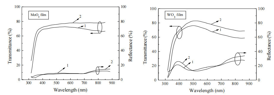
Optical transmittance was measured for the single oxides and the mixed oxide films. The results are shown on figure 1. It is seen that after annealing the transmittance of single oxides increases, while for the mixed WO3-MO3 it decreases. A possible explanation is mass transfer starting during annealing at elevated temperatures, but the process is not accomplished (annealing time was accepted to be one hour), the structure gets disordered, amorphous-like and the transmittance drops down.

Fig1
XRD patterns of MoO3, WO3 and MoO3 -WO3 films, deposited on conductive glass substrates are presented on figure 3. Most of the XRD lines found can be assigned to the corresponding oxides. MoO3 film consists of orthorhombic Mo trioxide and a small fraction of sub-oxide. The triclinic WO3 phase is prevailed in the tungsten oxide film with W20O58 sub-oxide. The XRD spectrum of the mixed oxide film is very similar in shape to that of WO3. Similar effect is observed for IR spectra. The XRD peak positions are the same with enhanced intensity, which leads to suggestion that W atoms are partly substituted by Mo atoms.
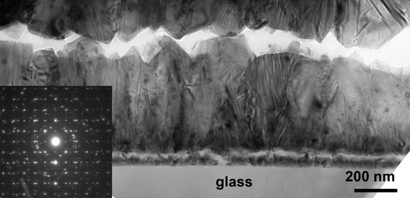
Figure 4 presents high resolution TEM micrograph of CVD as-deposited MoO3-WO3 film, grown at gas flow ratio 1/32. The columnar structure of the film is clearly observed, it is typical for the CVD grown films at temperatures below the melting point of the film material. These columns form grain boundaries which facilitate the ions intercalation.

Fig4
Cyclic voltammetry is used as method to study insertion reactions and to receive information about the electrochemical effects. Cyclic voltammetric experiments were performed in a standard threeelectrode arrangement. The electrodes were immersed in electrolytes of 1 mol/l LiClO4 in propylene carbonate (PC). Current density vs. voltage voltammograms were registered between -1 V and +1.5 V. The cyclic voltammetric (CV) curves manifest that the as-deposited and annealed MoO3-WO3 films.
上一篇: APCVD法生长的硅纳米线的化学表面钝化
下一篇: HF溶液中硅蚀刻过程中银的双重作用