Background
By etching silicon in a HF aqueous solution, porous silicon can be formed. When silicon etching in the HF solution is assisted by silver, well-organized nanostructures like silicon nanowires [1-3] are formed. The latter are very interesting in electronic and photovoltaic application. In order to enable significant improvements in the devices’ technologies, understanding of the fabrication mechanism must be attained to produce materials with precise control. Herein, we are interested in the silverassisted chemical etching of silicon in HF solution. This technique can be realized either by a one-step process or a two-step process. The one-step method includes, at the same time, metal deposition and electroless etching. In this process, the silicon substrate is immersed in an AgNO3/HF aqueous solution. The two-step method consists first of metal deposition and second, the chemical etching. In the latter method, the silver particles are evaporated or chemically formed on the surface of the silicon sample then introduced in a HF aqueous solution. With these two processes, we obtain two different behaviors of the silver particles; in one case, the silver catalyzes silicon, and in the other one, it protects the silicon underneath. Therefore, using a scanning electronmicroscopic (SEM) characterization, we tracked silver particles during silicon etching to determine which mechanism is privileged. To interpret the obtained results, we analyze charge displacement at the metal/Si interface. The developed model clarifies the role that the silver has during silicon metal-assisted etching experiences. Hence, the controversy regarding this role is solved.
Methods
For cleaning, samples were boiled in acetone for 10 min, followed by their immersion in ethanol for 5 min to remove organic greases. Then, we rinsed them three times with deionized water. Finally, samples were dipped in a 5% aqueous HF solution for 1 min to eliminate native silicon dioxide. This study was realized at two ambient conditions: room temperature and atmospheric pressure. The etching duration was 1 h. We used high purity single-crystalline silicon. The wafers are p-type, borondoped and (100)-oriented, with a thickness of 525 μm and a resistivity of 1 to 10 Ωcm. The samples were then separated in sample A and sample B to be treated differently. Sample A was immersed in an etching solution composed of HF/AgNO3 [1-3]. The concentrations in the latter were 40% and 0.02 M, respectively. On sample B, we first evaporated a 30-nm silver film, and then it was immersed in a 40% HF aqueous solution [4].

Fig1
Results and discussion
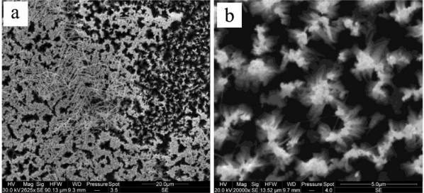
In Figure 1, we give the top section SEM images of sample A, where the silver nanoparticles cover the top surface of the SiNWs. The silver film formed on wafer A is not uniform and not compact. The nonhomogeneity of this film can be attributed to the surface status. It was reported in several works [5-7] that the dendrites formation is related to the electrons’ exchange between silicon atoms and silver ions. In Figure 1a, we observe in some regions silver nanoparticles on top of SiNWs, where the image in Figure 1b is the magnification of this zone. In other regions, the silver forms a filament-like structure. The growth mechanism of silver dendrites is still unclear; the diffusion-limited aggregation theory [8] may play an important role to explain this mechanism.
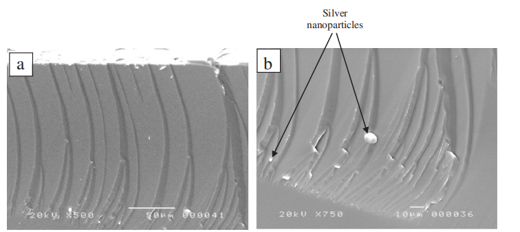
However, in the case of sample B, where a 30-nm silver film was deposited before the etching step, we observe pores formation at a depth of 200 μm as shown in Figure 2. Figure 2a is a tilted SEM image of the sample showing both the top surface and the cross section. We notice the beginning of pores from the top of the wafer and the presence of silver nanoparticles in the bottom of pores which is magnified in image (Figure 2b). The formed pores are not uniform. Hence, we observe the pores at different depths. The average of the pore diameters is around several micrometers. This could be due to the thickness of the silver film.

Fig2
From the obtained results for samples A and B, we estimate the etching rate for sample A at about 0.5 μm/min and the penetration rate of silver particles for sample B at about 2.7 μm/min.
The electroless metal deposition mechanism was presented by Morinaga et al. with copper particles [10]. Then Peng et al. started with the protecting mechanism that silver has during the silicon etching in the one-step method [1]. After that, they provided in [11] their new position regarding the etching processes of silicon wafers in aqueous HF/AgNO3 solution where the catalyzing effect was described. Qiu et al. [12] gave experimental evidences that silver protects the silicon underneath. Consequently, the role that silver has was still not elucidated.
In this section, we give the explanation of SEM images in Figures 1 and 2. Therefore, to understand the etching process of samples A and B, we propose a unique interpretation of the experimental observations in both cases by analyzing what happens at the silver/silicon interface. In Figure 3, we give the schematic band structure at the silver/silicon interface. In such a case, the work function of silver (ϕAg = 4.3 eV) is less than that one of silicon (ϕSi = 4.9 eV). Consequently, at contact, electrons diffuse from the metal to the semiconductor until the thermodynamic equilibrium is reached at the same Fermi level.
Conclusions
During metal-assisted etching experiences, some researchers reported that silver protects silicon. However, others confirmed that silver catalyzes the silicon underneath. In this paper, we give experimental results arguing the dual role that silver has during silicon etching. We propose a model based on the effect of electron transfer at the silver/silicon interface when silver is deposited during the HF etching (one-step method) and when silver is deposited prior to the etching in a HF solution (two-step method). By the proposed model, it becomes clear how silver nanoparticles can protect the silicon underneath in some experimental conditions and how they initiate pore formation by etching silicon underneath in others.
上一篇: APCVD过渡金属氧化物
下一篇: 微电子应用中的旋涂技术