ABSTRACT
Mid-infrared (mid-IR) absorption spectroscopy based on integrated photonic circuits has shown great promise in trace-gas sensing applications in which the mid-IR radiation directly interacts with the targeted analyte. In this paper, considering monolithic integrated circuits with quantum cascade lasers (QCLs) and quantum cascade detectors (QCDs), the InGaAs−InP platform is chosen to fabricate passive waveguide gas sensing devices. Fully suspended InGaAs waveguide devices with holey photonic crystal waveguides (HPCWs) and subwavelength grating cladding waveguides (SWWs) are designed and fabricated for mid-infrared sensing at λ = 6.15 μm in the low-index contrast InGaAs−InP platform. We experimentally detect 5 ppm ammonia with a 1 mm long suspended HPCW and separately with a 3 mm long suspended SWW, with propagation losses of 39.1 and 4.1 dB/cm, respectively. Furthermore, based on the Beer−Lambert infrared absorption law and the experimental results of discrete components, we estimated the minimum detectable gas concentration of 84 ppb from a QCL/QCD integrated SWW sensor. To the best of our knowledge, this is the fifirst demonstration of suspended InGaAs membrane waveguides in the InGaAs−InP platform at such a long wavelength with gas sensing results. Also, this result emphasizes the advantage of SWWs to reduce the total transmission loss and the size of the fully integrated device’s footprint by virtue of its low propagation loss and TM mode compatibility in comparison to HPCWs. This study enables the possibility of monolithic integration of quantum cascade devices with TM polarized characteristics and passive waveguide sensing devices for on-chip mid-IR absorption spectroscopy.
KEYWORDS
mid-infrared, absorption spectroscopy, quantum cascade devices, subwavelength waveguides, photonic crystal waveguides, photonics integrated circuits, parts per billion, gas sensing.
Another important consideration is the optical path length that can be accommodated on a lab-chip to enable suffiffifficient absorbance of the mid-IR light by the sensed analyte. Previously, it has been demonstrated that slow-light-enhanced two-dimensional (2D) photonic crystal waveguides (PCW), slotted PCWs (SPCWs), and holey PCWs (HPCWs) can effffectively reduce the optical absorption path length due to the slow-light effffect and increase the light−matter interaction length by enhancing the in-plane evanescent optical mode overlap within the low-index etched holes of the photonic crystal lattice.26−31 Our previous research elaborated that the peak electric fifield enhancement factor in the SPCWs was better than that for the HPCWs; on the other hand, the propagation losses for the HPCWs were 3× lower than those for the SPCWs.29 In recent years, subwavelength grating waveguides, or subwavelength meta-material clad waveguides, defifined by a periodic array of rectangular holes bordering a strip waveguide, have been proposed as effffective ways to ameliorate the cladding limitations, when appropriate highindex core materials are available.14−17,32−35 It is known that subwavelength gratings (SWGs) act as an effffective homogeneous medium with a spatially averaged refractive index.33 Moreover, as a subcategory of one-dimensional (1D) PCWs, it has been studied that SWG waveguides generate slow light by way of periodically modulated structures along the propagation direction with a higher group index than conventional strip waveguides.32−35
DEVICE DESIGN
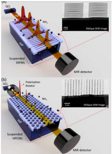
As our fifinal targeted device is based on the homogeneous integration between QCL/QCDs and passive waveguides.beneath them, the epitaxial material structure for this work is chosen considering effiffifficient light coupling between these components. In our previous research, we addressed and demonstrated all fundamental methodology and device integration steps, including monolithic epitaxial growth of the QCL/QCDs and compact integrated passive components’ fabrication feasibility.36−40 Several important remarks are described in the Supporting Information. Figure S1 shows the schematic of fully integrated monolithic sensors with QCL/QCDs and suspended waveguide passive sensing device; also, the cross-sectional SEM images of suspended HPCWs and SWWs are shown. With regard to the structure of QCL/ QCDs and PRS, the epi structure comprises an InP substrate with 1.15 μm InGaAs waveguide core layer targeting λ = 6.15 μm operating devices.37−39 Figure 1a,b shows a schematic ofsuspended SWW and HPCW devices that shows their structures and working characteristics with the corresponding SEM images. Detailed design principles for each device are described below.

Fig1
RESULTS AND DISCUSSION
Since the whole fabrication process is the same for HPCW and SWW devices, we utilize one wafer to fabricate both HPCWs and SWWs. Figure 4 shows scanning electron microscopy (SEM) images of a fabricated device. Figure 4a,b shows top views of the suspended HPCWs and SWWs, respectively. Figure 4c,d shows 90° bend with 50 μm bend radius and 180° bend with 30 μm bend radius, respectively. Cross-sectional SEM images of each device can be found in Figure S1 (inset) and in Figure 1a,b. We can see that the waveguide membranes are fully suspended without upper or lower cladding, and the air gap depth under the waveguides is more than 20 μm, which is enough to avoid mode penetration to the substrate. Despite this considerably deep undercut etch, top-view and crosssectional SEMs indicate robustness of suspended InGaAs structures showing no sag or bends even after cleaving.
Measurement Results.
By measuring the output power versus time, in the presence and absence of ammonia flflow from a calibrated Kintek vapor generator, we could evaluate the ammonia sensing performances of HPCWs and SWWs. We experimentally measured the background noise level of ∼0.09 dB, which is equivalent to ∼2% output signal changes in our measurement setup. We also measured the propagation lossesof both the suspended HPCW and the SWW by the cutback method as 39.1 and 4.1 dB/cm, respectively.
上一篇: GaN的湿法化学蚀刻
下一篇: 石英抛光方法