I. INTRODUCTION
Although the chemical reaction is well known, the anisotropic etching of Si in alkaline solutions is a complex process. This is particularly true in the solar industry where a large mass of silicon is typically introduced into the etch bath. The etch by-products (silicates) affect the balance of the etching specie. If adequate compensation is not made for these by-products, a significant drop in etch rate and an increase in contamination levels is typically noticed. As a result of this contamination, production lines would suffer from unpredictable wafer characteristics and hence lower cell .
In order to obtain stable and reproducible manufacturing processes, a reliable and accurate real-time measurement of the etching constituents becomes necessary. In addition, a mechanism by which fresh chemicals can be added to the etching bath is also required. The presence of these etch byproducts has been shown to slow down the etch rate even when chemical concentration is correct. Simply put, the solubility of etch by-products decreases once the concentration of silicates increases. And hence, Si mass transport from wafer surface to the etching solution is impacted. Chemical mixtures involved in solar cell manufacturing generally include: KOH/IPA, HF/HNO3, HF/HCl, and other compounds. Additives, e.g. surfactants, are typically used to enhance etch uniformity.
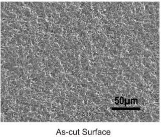
In this study, wafers were processed in a KOH/IPA mixture to produce texturized surfaces as shown in Figure 1. In-line sensors were installed to monitor the chemicals' concentrations in real-time. Algorithms were developed to control the chemical concentration by injecting fresh chemicals and water at a desired time interval to compensate for the loss of chemicals and water. The system also allows for draining and replenishing chemicals and water to keep the silicates under a threshold to maintain consistent etching characteristics under different bath loading conditions.

Fig1
II. EXPERIMENTAL
Wet chemical processes were conducted on a fullyautomated GAMASolar™ wafer etching and cleaning station. The batch size was 200 wafers per run. All tests were performed with the same wafer supplier, including wafers from about 100 different ingots. Silicon etching processes were conducted with the aid of Akrion Systems' patented in-situ chemical concentration control system (ICE-1™). Measurements of concentrations were taken using inline NIR (near Infra-Red) sensors installed in the recirculation loop of the process tanks. These sensors measure light absorbance and transmit it through fiber optics cables to an array of detectors (spectrophotometer).
The light absorbance of given specie in the solution is correlated to its concentration over a wide range of wave lengths. The signal is then reported to an amplifier that scales the response to a 4-20 mA output. This signal is subsequently fed into an analog module that scales the signal and reports directly to the system computer which controls the spiking (volumes and frequency) of chemicals to maintain concentration. A variety of chemicals e.g. HF, HNO3, HAc and applications were also studied but only the results of KOH/IPA control will be presented here. The goal was to produce consistent etch rates and texturization patterns similar to those shown in Fig. 1 over the entire bath life and different silicon loading levels.
III. RESULTS AND DISCUSSION
This technology provides technical advantages by accurately measuring the concentration of chemicals to produce the desired process results - in this case the texturization pattern [1-3]. Controlling concentration for uniform, repeatable texturization will help solar cell manufacturers reduce cost of ownership (COO) and overall cost of manufacturing by extending the usable life of the chemical bath, which in turn extends the up-time and overall utilization of the tool [4-5].
上一篇: 硅晶片的酸刻蚀