Scope
Diamond and Related Materials is an international, interdisciplinary journal which publishes articles covering both basic and applied research on diamond materials and related materials. These include cubic boron nitride and materials with characteristics and properties approaching or possibly exceeding those of diamond.
The primary emphasis is on vapour-deposited materials; also important are high-temperature/high-pressure synthetic materials, as well as relevant natural diamond research and characterization. Papers published cover all fundamental and technological aspects of synthesis, characterization, properties, devices and generic applications of these materials.
Advertising Information
Advertising orders and enquiries may be sent to: International: Elsevier Science, Advertising Department, The Boulevard, Langford Lane, Kidlington, Oxford OX5 1GB, UK. Tel.: +44 (1865) 843 565. Fax: +44 (1865) 843 952. USA and Canada: Weston Media Associates; Dan Lipner, P.O. Box 1110, Greens Farms, CT 06436-1110, USA. Tel.: +1 (203) 261 2500. Fax: +1 (203) 261 0101. Japan: Elsevier Science Japan, 9-15 Higashi-Azabu 1-chome, Minato-ku, Tokyo 106; Tel: +81-3- 5561-5032; Fax: +81-5561-5045.
Preface
The first European Conference on Silicon Carbide and Related Materials (ECSCRM 96) was held in Heraklion, Crete, Greece from October 6 to October 9, 1996. This was the first event of a series of biannual conferences addressing wide band gap semiconductors research field and supported by the European Union through the "Euroconferences" action. The next conference will be held in Montpellier, France in 1998.
The conference was attended by 140 scientists from 13 countries representing most of the European research groups active in the subject. Thirteen invited talks, 18 oral and 61 poster contributions were presented in 8 oral and 2 poster sessions. These 92 contributions demonstrated the rapid development of wide band gap semiconductor research. Moreover, two panel discussions on European effort on SiC wafer production & SiC bulk and epitaxial growth apparatus and on SiC-based devices and applications were organized.
1. Introduction
As the field of SiC grows, the task of reviewing in a very limited space becomes harder and harder. We have chosen to start where our last review stopped [1]. Only a few selected topics have been chosen with the full knowledge that other equally interesting contributions have been left unmentioned. We apologize for having had to pick and choose, and fully recognize that our selection was biased by our own interests.
2. VUV reflectivity and band structure of SiC
It has been recognized for a long time that the occurrence of as many as 170 polytypes of SiC leads to strong differences in many of the properties of these polytypes. A striking example is the variation of the minimum indirect band gap from 2.42 eV in 3C SiC to 3.33 eV in 2H SiC, as well as the notable changes in the locations of the conduction-band minima. In recent years there has been substantial progress in SiC boule growth for substrates which are subsequently used for epitaxial growth of relatively thick and perfect layers of single-crystal material. This development enables one to obtain sufficiently large samples for absolute reflectivity measurements in the vacuum ultraviolet. More importantly, the epitaxial layers have flat specular surfaces in "as-grown" form. This is critical, since polishing introduces surface damage which can seriously perturb the reflectivity results in the ultraviolet due to the very small penetration depth of the light into the surface. With good "as-grown" surfaces in hand, a systematic VUVreflectivity (4-10 eV) investigation of the polytypes 3C, 4H, 6H and 15R SiC was conducted [2-4]. In parallel with the experimental study, a series of band-structure and optical response function calculations was carried out and used to interpret the data. The reflectivities of 3C, 4H, 6H and 15R SiC were found to have significant differences. The positions of all major features are in good agreement with those obtained from density functional theory (DFT) calculations in the local density approximation (LDA) using the scalar-relativistic linear muffin-tin orbital (LMTO) method in the atomic sphere approximation (ASA) modified by a polytype- and energy-independent upward shift of the conduction bands, which at the same time provides good agreement for the minimum band gaps. The major peaks in the reflectivity are associated with relatively extended areas of nearly parallel bands at general k points, and not with critical point transitions at symmetry points. The trend of minimum and specific A-point band gaps of five polytypes of SiC with hexagonality has been discussed.
It is the aim of the present paper to give through an analysis of the results obtained so far on the crystal growth of 6H-SiC some indications about the relations between growth conditions and defects formation.
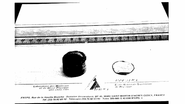
Fig. 1 shows a typical 25 mm diameter and 10 mm height single crystal 6H-SiC boule grown by this process together with a nitrogen doped polished wafer cut from the boule.

Fig1
The polytype identification was made by X-ray diffraction, Raman spectroscopy and photoluminescence at low temperature. The crystal defect densities and distribution were assessed by optical and scanning electron microscopy on samples chemical etched in molten KOH at 500°C for 15 min in order to distinguish between dislocation pits, micropipes, low angle boundaries between grains and inclusions. The existence of domains with small disorientations was studied by high resolution X-ray diffraction and X-ray topography in transmission geometry using polychromatic (white beam) synchrotron radiation [21]. These measurements were carried out at ESRF-D5 optics beamline.
下一篇: 晶圆级芯片封装可靠性的提高