1. Introduction
Silicon nitride (SiN) thin films are widely used in various microelectronic and optoelectronic devices (Ino et al 1994). It is used as gate dielectric in MOS components (Tsividis 1999) and also applied in the fabrication of microelectromechanical systems (MEMS) (Kaushik et al 2005). In photovoltaic field, SiN has the function of defects passivation (Sopori et al 1996) and light antireflection (Barreraa et al 2008). SiN is applied as antireflective coating (ARC) to minimize reflections and ensuring a higher photocurrent (El Amrani et al 2008). It is also known that the hydrogen introduced in SiN film has a crucial role in the bulk and surface passivation (Duernickx and Szlufck 2002; Sopori et al 2005). Generally, for solar cells metallization a standard screen printing process is applied. Initially, this process was first developed for monocrystalline silicon solar cells and then adapted for multicrystalline silicon substrate. The application of this process on mc-Si wafers results in lower performance solar devices. A classical hydrofluoric acid (HF) dipping is well known for enhancing the efficiency (η) and the fill factor (FF) and for long time was applied on monocrystalline silicon solar cells. Unfortunately, HF immersion was found to be less effective in enhancing the electrical characteristics (η and FF) of the mc-Si solar cells. By contrast, we show in this paper that we can boost mc-Si solar cells performances with our new and cost effective chemical H3PO4 treatment.
2. Experimental
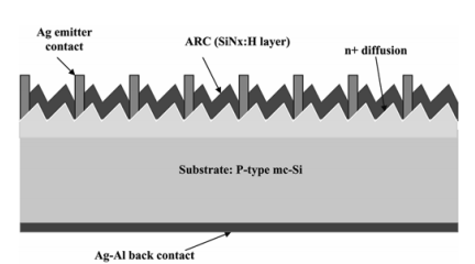
Solar cells used in this study were based on structure of n+ /p junction. The structure of this n+ /p multicrystalline silicon cell is given in figure 1.
The starting material was a mc-Si wafer of p-type (boron-doped) with ~ 3 Ω cm resistivity and having an initial thickness of 380 μm. These wafers were dipped into NaOH (30% at 85°C) polishing solution until a final thickness of 350 μm was reached; followed neutralization and RCA decontamination stages by putting them in a bath made of H2O2/NH4OH/DI H2O at 70°C, then etched in diluted HF (5%) immediately (Kern and Puotinen 1970).
3. Results and discussion
The H3PO4 treatment was applied to n+ /p standard solar cell that has been realized by the process described above. Conceding that, the initial efficiency (η) and fill factor (FF) were as low as 5⋅4% and 50⋅4%, respectively for sample S1. Nevertheless, after H3PO4 treatment for 30 min at 85°C, we observed an improvement of η and FF as shown in figure 2. The η reached 7⋅7% and FF 70⋅8%, this means a relative increase of about 40% up from the initial values. In order to demonstrate the reproducibility of this process we have etched a second sample (S2). Figure 3 shows the amelioration of η and FF. For the S2 solar cell, we have chosen the etching times: 10, 20, 30 and 40 min. Series resistance was calculated and found to be decreasing after chemical attack as shown in figure 2. In order to understand the physics behind the boosting of η and FF, we made a full analysis of the chemical composition of SiN thin layer before and after etching.
4. Conclusions
We have shown an effective amelioration of I(V) characteristics resulting from a new H3PO4 chemical treatment. A boosting up to 40% of efficiency and fill factor has been successfully accomplished by this treatment. AFM study shows that SiN layer is starting to be locally etched after 30 min of H3PO4 etch which facilitates the acidic solution penetration to the SiN/Si interface. Thus, the passivation by hydrogenation becomes more probable. Finally, SEM–EDX study showed that after this chemical treatment, the rate of Si content increases in all regions (small grains, large grains and grain boundaries) of the SiN thin layer and thus ameliorating the passivation effect. Phosphoric acid passivation is an effective way to make a better passivation of SiN/mc-Si interface at low temperature.

Fig1
Finally, we used a Varian Cary 500 spectrophotometer to extract the reflectance of thin SiN layer. The reflectance was measured for each of the samples that were etched for different times. We can see from figure 7 that a non-etched SiN layer is highly reflective in the visible range as well as the near-UV. In contrast, the sample etched for 25 min displays a low reflectance behaviour in the near-UV range. The sample etched for 15 min in H3PO4 possesses the best reflective characteristics in the 400–700 nm range i.e. it absorbs more light than the other samples on a broader spectral array.
上一篇: 生长宽带隙半导体氮化铝晶体的环保方法
下一篇: 磷酸电解液中铜电解抛光的机理研究