I. INTRODUCTION:
Controlling the morphology of semiconducting nanostructures is the most important parameter for optical-electronic technological applications.1 ZnO, with band gap of 3.3 eV has a wurtzite crystal structure and high exciton binding energy of 60 meV.2,3 It has received lot of attention as a nanostructured material due to its unique properties related to numerous applications, such as in opto-electronic devices (light emitting diodes (LEDs), laser diodes, solar cells, photodetectors), energy harvesting devices (Nano generators), electronic devices (transistors), sensors, catalysts, piezoelectric etc. 4 Despite rising evidence of significant Eco toxicity it is often regarded as non-toxic and biocompatible,5 its synthesis does not require toxic precursors.
A number of studies on the preparation technique of ZnO nanostructure are reported using wet chemical, electro-deposition, template assisted route, thermal evaporation, chemical vapor deposition (CVD) techniques, most of these techniques require sophisticated instruments to generate high temperature or high pressure. Wet chemical is the most simple and cost effective technique to prepare highly crystalline ZnO. To further ensure economically cheap technique, we have used amorphous glass substrates for the synthesis of nano structure. But the true challenge lies in the synthesis conditions which control the crystal growth in a particular fashion to grow desired nanostructures moreover prevention of cluster formation. Previously, this complex growth mechanism is mostly explained based on catalyst-driven mechanisms (solution-liquid solid6,7 and vapor-solid-solid8 growth) and vapor-liquid-solid (VLS)9,10 mechanism. But recent studies show that axial screw dislocation mechanism drives the spontaneous formation of nano-wire/tube structure.11,12 Size and morphology plays a vital role in the physical properties of the nanomaterial. So here, we have focused on the variation of optical properties with the change in shape and size of ZnO nano structures.
II. EXPERIMENTAL TECHNIQUE:
A. Synthesis process
Zinc Acetate dehydrate (Zn (CH3COO)2. 2H2O) (100mM: Alfa Aesar chemicals) is used as the precursor for preparation of pure ZnO films on glass substrate by the most simple and inexpensive hydrothermal method on a large area at atmospheric pressure. An aqueous solution of Zinc Acetate is prepared in a 100 ml double distilled water as starting material. After complete dissolution of chemicals in distilled water, ammonia is added drop wise to form resultant solution with a pH∼13. The substrates are cleaned first with distilled water, followed by Acetone and Ethanol by ultra-sonication for 10 min in each solution and air dried. Glass substrate is kept vertically in the solution. To understand the growth mechanism more clearly, reaction time (120 min) was kept constant and reaction temperature is varied from 70 ◦C to 120 ◦C. Deposited films are taken out from the solution and washed with distilled water for several times to remove over deposited/ ammonia related impurities from the film. Dried films are annealed in air at 150 ◦C for 2 hrs to obtain pure phase ZnO.
III. RESULTS AND DISCUSSION
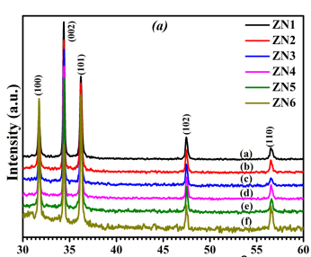
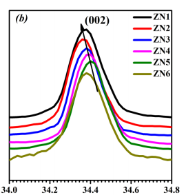
Figure 1 shows the XRD pattern of ZnO nano-structure deposited on glass substrate at different deposition temperatures keeping deposition time constant (120 min.). All major peaks (2 ⊖ ∼ 30◦ to 60◦ ) can be assigned to the pure hexagonal phase of wurtzite-type ZnO structure with space group P63mc. Fig 1(a) shows that at such a low synthesis temperature a highly crystalline and pure phase of ZnO has been obtained. The film grown below 120◦C shows a more preferred orientation along (002) planes in comparison to powder samples where (101) planes have the strongest peak intensity.13 However the nano-material films grown at 120 ◦C, shows a reduced relative intensity of the (002) reflection, disappearance of (00l) plane is might be due to the change in structure.14 Fig 2(a) shows Reitveld refinement plot of ZnO deposited at 90 ◦C using “Fullprof” software. Refined lattice parameter value of the nano structures are shown in Fig. 2(b).


Fig1(a) Fig1(b)
To check the plausible mechanism of ZnO nanostructures, we performed the experiments at fixed deposition temperatures (at 70 ◦C and 120 ◦C) and varied the deposition time at the interval of 30 min and deposition was carried out at 30 min, 60 min, 90 min and 120 min. Fig. 5 shows of FESEM images of films deposited at 70 ◦C for 30 min -120 min in (a-d) and 120 ◦C for 30 min -120 min from (e-h), it noticeably visible that the rods and tubes synthesized at different temperature and time evidenced screw dislocation mechanism as reported by Yang et al., Jin et al. and Bierman et al. 20–22 Screw dislocation mechanism might responsible for modification of rods into tubes as reported by Yang et al., Jin et al. and Bierman et al. 20–22 Also one cannot rule out layer by layer deposition in these rods and tubes as from the side view of the rods and tubes one can obviously realize the layer like structure.23
Simple technique for the highly-ordered growth of ZnOnano-flowers, nano-rods and nanotubes films on glass substrates by controlling merely growth temperature is established. The XRD studies indicate the films are highly c-axis oriented. Reitveld refinement confirms the first decrease in the lattice constant until growth temperature 110 ◦C and then increase for 120 ◦C, even though it is small. The FESEM images clearly indicate the change in the ZnO morphology with synthesis temperature, at lower temperature (7 ◦C) needle flowers, at (80-110 ◦C) rods-flowers and at (120 ◦C) tube formations evidenced. The possible growth mechanism of needles, rods and tubes are elucidated. Depending on the morphologies naturally band-gap was found to contrast. PL data indicates the intensities and defect levels changes with synthesis temperatures too. The presence of defects formed in highly non-equilibrium conditions had a significant impact on the luminescence of ZnO. We demonstrated a superior control not only on the morphology but also on the defect levels for nano-rods/tubes by controlling synthesis temperature. Such ample defect level adjustments will greatly benefit the applications of ZnO nano-needles/rods/tubes in light emission, opto-electronic devices, biological labelling, display devices, etc.
下一篇: ZnO 的湿化学表面纹理化