I would like to express my sincerest gratitude to my main supervisor, Dr Tan KayChen, my co-supervisor, Dr Arthur Tay and Dr Ho Weng Khuen, for their acad-emic direction, guidance and support throughout the course of this work. All I havelearned is based on their combined knowledge of system identification and semicon-ductor manufacturing process.
stress by heating processing (e.g. thermal oxidation, rapid thermal processing(RTP), bake process in lithography) also cause wafers to bend. The mismatch in thecoefficient of thermal cxpansion among different layers in silicon substrates inducessome distortion at the wafer level; In general, in the process of heating, the temper-ature of center of wafer is higher than that of edge of the wafer. The temperature uniformity for large wafer size is hard to achieve due to the complex thermal dynamicsthe hotplate experience and other disturbance. The mechanical stress arising fromthis temperature variation cause the warpage or bow of the wafer.
In lithography process, measurements of the material at selected points throughoutthe process are an essential part of the preparation of wafers 7 . From crystal andwafer shaping through the final wafer finishing steps, measurements are required forquality control, for meeting customer specifications, to correct problems before theycreate scrap material and to avoid further processing of reject material. The typesof mcasurement nceded depends to a large xtent upon the specifications required by the use, however other considerations relating to cost, product improvement effortsand reliability of the test will also go into the choice. Provided the selection ofmeasurement techniques is made with care, the cost of the in-process measurementis fully justified by the benefits. With in-process measurements, the process canbe controlled in real time, as input and control parameters are adjusted accordingto the fluctuations present in the readings of the sensor. Moreover, with in-processmeasurement, there is no additional process steps that is needed in addition of theoriginal system processing steps.

Fig1
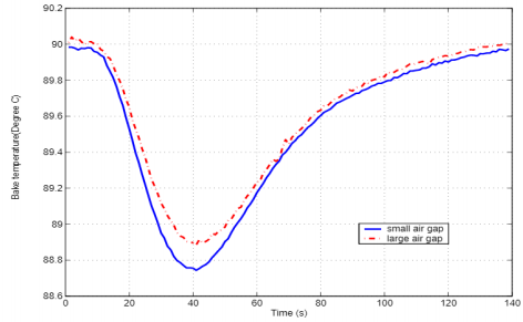
In summery, the four bake processes involved in the lithography process was intro-duced and the industrial standard for measurement of wafer warpage is presented, andthe advantage and the method of our warpage estimation have been shown. We couldgain some intuition about the feasibility of our proposed methods by comparison thetwo diagrams we get from the experiment.
下一篇: 辅助陶瓷蚀刻的超声加工