Smaller, faster and smarter electronic equipment is coming to the world every dayHowever, people are never satisfied and semiconductor technology has to face manydifficult challenges as we enter the 21 century. According to Moore's Law, whichstates that device complexity doubles about every 18 months, among many challengesthe feature size needs to be reduced to approximately 1.4 times for every generation. Forfuture sub-0.1 am MOSFET, new type of MOSFET structures or new materials arerequired. A scaled MOSFET (Metal Oxide Semiconductor Field Effect Transistor)requires a thinner gate, different gate materials and very shallow source/drain junctions.When the gate length is reduced to less than 0.l om, an extremely shallow source/drainjunction of less than 40 nm is needed to suppress the short-channel effect. Furthermore,the shallow junction also needs to be highly doped for series resistance reduction. Verylow-energy implantation could result in highly doped shallow junctions. However, theseshallow junctions suffer from implantation damage. As a result, the junctions becomemuch deeper after the annealing process due to transient enhanced diffusion. Diffusionfrom highly doped spin-on glass - SOG (or spin-on dopant - SOD) is one of thealternatives.
Shallow junction formation using SOD is the subject of this thesis. Very shallowjunctions of less than 20 nm have been realized using spin-on dopant diffusion into SiThe diffusion of impurities from SOD into polysilicon on silicon structure was alsoinvestigated. Very high quality shallow junctions with low sheet resistance wereobtained by this technique. The results were published and a poster of this subject wasawarded as best poster for a scientific contribution in the 1st annual BENELUXworkshop on “Semiconductor Advanced for Future Electronics” in Mierlo. theNetherlands(1998).
The technology of sol-gel thin film has been around for over 20 years and is now wellaccepted as a technology for forming thin films and coatings. The process is simple, asolution containing the desired oxide or non-oxide precursor is prepared and is appliedto a substrate by spinning, dipping, draining or spraying. The process is able to apply acoating to the inside and the outside of complex shapes simultaneously. The films aretypical a few hundreds of nanometers thick, uniform over large areas and adherent. Theequipment is inexpensive, especially in comparison to any deposition technique thatinvolves vacuum. Coatings can be applied to metals, plastics, and ceramics. Typically.the coatings are applied at room temperature, though most need to be calcined andcondensed by heating. Both amorphous and crystalline coatings can be obtained. Thereare many useful applications of sol-gel technology such as coating for optical,electronic, sensor, abrasion, barrier, protective, and catalyst applications. In some casesthe quality of the coatings obtained by the sol-gel process is limited in comparison tooxidation, evaporation or sputtering techniques. Furthermore, the shelf-life of sol-gelsolutions is limited to typically 12 months.

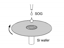
Fig1
In the systemms described above, the sol-gel transition is reached when one-phase liquidbecomes a two-phase alcogel, solid plus liquid. The alcogel is an oxide polymer thatcondenses in the presence of solvent. Alcogel is used to differentiate gels prepared withalkoxides from those prepared from ion-exchanged solutions or colloidal sols. Thosegels are called hydrogels. The transition in alcogels is irreversible and occurs with nochange in volume. The time of the transition depends on the chemistry of the solution.but the chemical composition of the two phases at the transition is not unique. Oncethrough the sol-gel transition, the solvent phase is removed to create xerogels byordinary evaporation or aerogels by hypercritical evacuation. At this point, the dried gel1s a micro-porous oxide.