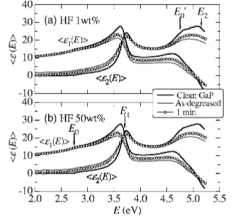
Chemically cleaned GaP(001) surfaces in aqueous HF solutions have been studied usingspectroscopic ellipsometry (SE),ex situ atomic force microscopy (AFM),x-ray photoelectronspectroscopy (XPS), wetability, and photoluminescence (PL) measurements. The SE data clearlyindicate that the solutions cause removal of the native oxide film immediately upon immersing thesample (≤1 min). The SE data, however, suggest that the native oxide film cannot be completelyetch-removed. This is due to the fact that as soon as the etched sample is exposed to air, the oxidestarts to regrow. The SE estimated roughness is ~1 nm, while the AFM roughness value is~0.3 nm. The XPS spectra confirm the removal of the native oxide and also the presence of regrownoxide on the HF-etched GaP surface. The wettability measurements indicate that the HFcleanedsurface is hydrophobic, which is in direct contrast to those obtained from alkaline-cleaned surfaces(hydrophilic). A slight increase in the PL intensity is also observed after etching in aqueous HFsolutions.@ 2007 American Institute of Physics.
Gallium phosphide (GaP) is one of the most importantIll-V semiconductors because of its applications to opto-electronic and high-temperature electronic transport devices.Because of its highly reactive nature, the GaP surface is eas-ily oxidized in room-temperature air with the formation of anative oxide film several nanometers thick. A clean materialsurface is absolutely essential for various semiconductor de-vice techniques.
A useful guide to references on wet chemical cleaninghas been given by Clawson19who presented some of theworks done on IlI-V semiconductors. However, the literaturediscussing on the surface cleaning of GaP is still limitedl7.18.only reports have been published on the chemical cleaning ofthe GaP surface in acidic (HC) (Ref. 17) and alkaline (KOHNH,OH) (Ref.18) solutions. No cleaning study in acidic HFsolution has been performed to date. In silicon technology,HF cleaning is well known to result in the removal of thenative oxide and leaves behind stable silicon surfaces termi-nated by atomic hydrogen.

Fig1
The GaPsamples used in this study were n-type Te-doped (001)wafers with resistivity ~0.15 cm. Thesamples were first degreased with organic solvents in an ul-trasonic bath and then rinsed with de-ionized water. No fur-ther cleaning of the sample surface was performed. Thesample surfaces to be studied were, then, covered with a~2-nm-thick native oxide film. Note that this value was de-termined by SE and thus the effective thickness, modeled asan equivalent dielectric layer of the GaP oxide. not the actualone.
上一篇: KOH和 HCl处理后氧化铟锡表面的表征
下一篇: 旋涂玻璃:先进 IC 技术中的材料和应用