The extraction of the light produced by an organic light emitting diode has been made possible by the use of transparent conductive materials which should have well defifined electronic and optical properties. All the requirements are satisfified by indium tin oxide which has rapidly become the most common conductive substrate used for the growth of organic light emitting sources. Atomic force microscope, conventional X-ray photoemission spectroscopy and scanning photoemission spectromicroscopy have been used to investigate the morphology and the chemical properties of commercial thin indium tin oxide fifilms after several treatments commonly used prior to the organic layer growth for smoothing/cleaning/patterning the surface. Unambiguous smoothing effffects of the potassium hydroxide-based solutions have not been observed while Si contaminations of the surfaces have been found after the application of difffferent patterning procedures. 2007 Published by Elsevier B.V.
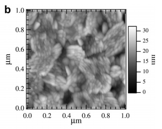
Here we present a systematic study of the chemical composition and topography of ITO commercial fifilms exposed to KOH etching for difffferent times and after the difffferent steps of the patterning process. Chemical composition has been investigated at two difffferent spatial scales: with conventional X-ray photoemission spectroscopy (XPS) averaging the probed area over few square millimetres and with synchrotron based Scanning Photoelectron Spectro-microscopy (SPEM) capable of 150 nm lateral resolution in order to detect chemical changes at microscopic level. The topography has been investigated by using the atomic force microscope (AFM) at a spatial resolution of 1 nm.
All the AFM images were made by a commercial NT-MDT Solver Pro microscope at the ELETTRA Nanostructure Laboratory. The instrument is furnished with a 50 50 5 lm closed loop scanner. The topographic images were done in contact mode using silicon rectangular cantilever (MikroMasch, spring costant: 0.6–1.0 N/ma) at a resolution of 256 256 pixels. A laser is focused on the back of the cantilever and deflflected to a four-segment photosensitive detector, which can monitor the vertical deflflection and the twisting of the cantilever as the tip scans across the surface. The height resolution during scanning was about 0.06 A˚ .


Fig1
The commercial pristine ITO fifilms here studied are characterised by a grainy structure with a grain size ranging from few to several tens of nanometer. The photoemission maps, despite their lower spatial resolution if compared with AFM measurements, clearly show a chemical heterogeneity of the surface; two distinct features can be identifified from the photoemission maps: few sub-micrometric well defifined C-rich spots and a smooth variation of the In content over the probed area visible also in the corresponding O map not shown here. The presence of the C-rich spots in the ITO fifilm surface can be attributed to contaminations of the raw materials used for the fabrication of the ITO or induced during the growing phase. A large sampling of the ITO surface has provided an indication of the density of the larger C-rich spots which is one spot every 20 20 lm2 . The variations of the In concentration over the surface are limited to few percent of the average value and could arise from a difffferent stoichiometry of the ITO or to difffferent atomic terminations of the grains.