Abstract: We present a proof-of-concept demonstration of a Ge/a-Si hybrid photonic integrated circuit platform utilizing a high-quality Ge-on-insulator (GeOI) wafer fabricated by wafer bonding technology. Amorphous Si (a-Si) formed by PECVD is found to be a promising alternative to conventional Si passive waveguides on a SiO2 BOX. Taking advantage of the high crystal quality of the Ge active layer and the easy fabrication of an a-Si waveguide, a low-dark-current Ge waveguide PIN photodetector monolithically integrated with an a-Si passive waveguide is successfully demonstrated on a GeOI wafer.
In recent decades, there has been significant progress in the field of Si photonics. Among them, the introduction of a Ge thin film into Si-based platforms has proved to be a successful approach, which enables not only new device functionalities but, more importantly, the realization of various advanced systems on a single chip [1–4]. Ge has many advantageous optical properties over Si. It exhibits strong optical absorption at wavelengths from 1.3 μm to 1.55 μm, making it ideal for photodetectors (PDs) in optical fiber communications [5–7]. A large electro-absorption effect has also been observed in Ge, making it promising material for realizing efficient optical intensity modulators [8,9]. Although Ge is an indirect-bandgap semiconductor similar to Si, its direct bandgap is only 0.14 eV above the indirect bandgap at the Γ valley. With the help of emerging band structure engineering technologies, it is even possible to fabricate practical Ge-based light sources [10–13]. Thus, by realizing Ge active photonic devices and Si passive devices, integration between Ge and Si provides a promising means of achieving a cost-effective highly functionalized photonic integrated circuit (PIC) platform, suitable for a wide range of applications.
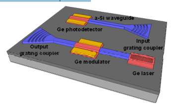
Figure 1 illustrates the concept of Ge/a-Si hybrid PICs built on a GeOI wafer. A Ge device layer with high crystal quality as well as strong optical confinement in the GeOI wafer fabricated by wafer bonding allows us to develop high-performance, low-power, and compact PICs for NIR wavelengths. In this paper, we present a proof-of-concept demonstration of a Ge/a-Si hybrid platform on a GeOI wafer. First, we investigate Ge waveguide PDs on a GeOI wafer. Then, monolithic integration between an a-Si waveguide and a Ge PD is achieved by applying an optimized integration process, showing the feasibility of GeOI-based PICs with a-Si waveguide interconnects for NIR photonics.

Fig1
For ease of measurement, a pair of focusing grating couplers is designed at both ends of the a-Si waveguide, following a similar design methodology to that for conventional SOI grating couplers [25]. Assuming the refractive index value of a-Si to be 3.7 [24], a grating pitch of 560 nm, filling factor of 0.5, incidence angle of 9° and etching depth of 70 nm are applied as the design parameters of the grating couplers with an a-Si layer thickness of 220 nm with the aim of achieving at a central wavelength of 1550 nm. In addition, grating couplers and Si waveguides are also fabricated on an SOI wafer containing a 220-nm-thick Si top layer and a 2-μm-thick SiO2 BOX for comparison.
上一篇: 硝酸浓度对多孔氧化锌薄膜刻蚀工艺能的影响
下一篇: KOH和 HCl处理后氧化铟锡表面的表征