In this work we present the results of experiments aimed at comparing the performances of various techniques for the detection of metal contamination in the silicon technology. Techniques for the measurement of surface contamination such as Total Reflection X-Ray Fluorescence (TXRF) and Time-ofFlight Secondary Ion Mass Spectrometry (ToF-SIMS) are compared with techniques for the measurement of contamination in the silicon volume, specifically the Deep Level Transient Spectroscopy and techniques for the measurement of carrier lifetime. Carrier lifetime measurements were obtained by photocurrent measurements and by Surface Photovoltage measurements.
In all these experiments, advantages and disadvantages of the different techniques are discussed. The results of this study clearly show that it is not possible to define a unique recipe that can be applied in all cases. The maximum tolerated contaminant concentration per unit area depends on the contaminant diffusivity, and is much lower for slow diffusers. The contaminant diffusivity and solid solubility in silicon determine the in-depth distribution of the contaminant, and hence the most effective approach.
Metal contamination in silicon has been studied for a long time [1], and the problem of detecting such contamination with the required sensitivity has been addresses by extensive studies [2][3]. The contaminant concentration per unit volume must be of the order of 1010cm-3 or less to guarantee the integrity of thin gate oxides [4]. In addition to the most common and most studied contaminants (e.g. iron and copper, [5][6][7][8]), new elements were introduced a few years ago into the fabrication process, for instance palladium to improve the wire bonding reliability [9][10]. Many common contaminants (for instance iron, nickel, copper, as well as palladium) diffuse via an interstitial mechanism in silicon, and are therefore fast diffusers [1], with diffusivity in the range 10-4-10-6 cm2 /s at 1100°C. These impurities easily redistribute through the whole wafer thickness during an ordinary thermal treatment for device fabrication. However, some metals (for instance molybdenum and tungsten) are slow diffuser contaminants, with diffusivities of the order of 10-9 cm2 /s or less at 1100°C. These contaminants were found to be detrimental for imager sensor devices even in very low concentration per unit area (down to 107cm-2).
The techniques for monitoring metal contamination can schematically be divided into two main branches, one consisting of the techniques that measure the chemical concentration at the silicon surface and the other of the techniques that measure the electrical activity of the contaminant in the silicon volume. Of course, the former approach is preferred when the contaminants are expected to be deposited at the wafer surface, and the latter for processes involving thermal treatments able to diffuse the contaminant in the silicon volume. Among the methods for measuring metal contamination at the silicon surface, the Total Reflection X-ray Fluorescence (TXRF, [14][15][16]) is probably the most commonly used, because it is sensitive to low contaminant concentration, non-destructive and compatible with the production line environment. Synchrotron-Radiation TXRF (SR-TXRF) is sometimes used to enhance the TXRF sensitivity and spatial resolution [17][18][19][20], or because it allows reference-free analysis [21], though of course it is unsuitable for systematic in-line control.

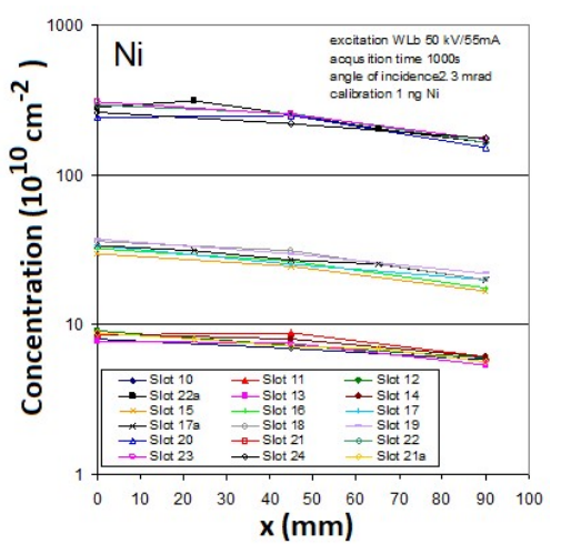
Fig1
DLTS measurements yield the contaminant concentration in the silicon volume, and requires the formation of a Schottky diode, so some more preparation is needed for DLTS samples. A RTA (1100°C, 3 min) was use to diffuse the contaminant in the silicon volume, then the arsenic doped layer was removed by Reactive Ion Etching (RIE) and 1000Å titanium was deposited, masked and etched to form the Schottky diode. This procedure was previously calibrated to measure the tungsten contamination in implanted wafers [43], so we can convert the tungsten concentration measured by DLTS in the silicon volume into tungsten concentration per unit area, to be compared with TXRF data.
A 1800 Å Si3N4 layer was deposited on the wafer surface, and the wafers were intentionally contaminated by contact with a contaminated chuck. A few bare wafers were contaminated with the same procedure for a comparison. The contaminant concentration deposited at the wafer surface was measured by TXRF. After contamination, some samples were cleaned (30 min or 60 min cleaning process) to test the efficiency of the cleaning procedure, and the wafers were thermally treated with a treatment typical of the final part of the process flow (340 °C, 90 min). This thermal treatment is used as the palladium drive-in, to investigate whether palladium can diffuse through the barrier layer in the silicon lattice. Finally the contaminated layer was removed and the wafers were annealed by RTP at 1100 ºC for 3 min to activate palladium for SPV measurements.
上一篇: 玻璃晶圆机械性能:与硅的比较