MICROLENSES and their arrays have many application possibilities in photonics in which devices and systems are ever decreasing in size. They are becoming popular for their ability to manipulate light in a miniature scale and to make the overall packaging simple and compact. Thus, it is anticipated that microlens applications in photonics will widely spread in a variety of formats. A good example is dense two-dimensional (2-D) microlens arrays integrated with vertical-cavity surfaceemitting lasers (VCSEL’s) and photodiodes for parallel data communications through free space [1]. Among others, refractive microlenses formed directly onto semiconductor materials draw much attention because they facilitate monolithic integration with other semiconductor optoelectronic devices, allowing a higher level of integration. Also, the high refractive index of semiconductor materials enables a microlens with large numerical aperture, enhancing the light capture efficiency.
The methods developed so far for semiconductor microlens fabrication include photoresist reflow followed by dry-etch [2], [3], mass transport after pre-shaping [4], and shadow mask regrowth [5]. However, those methods require multiple process steps (sometimes even at high temperatures) and/or expensive processing equipment, which are not generally compatible with cost-effective commercial production requirements. In this letter, we propose and describe a method to fabricate semiconductor microlenses in which only a simple one-step chemical etching process is involved. We also present experimental data to demonstrate the high quality of the processed microlenses.
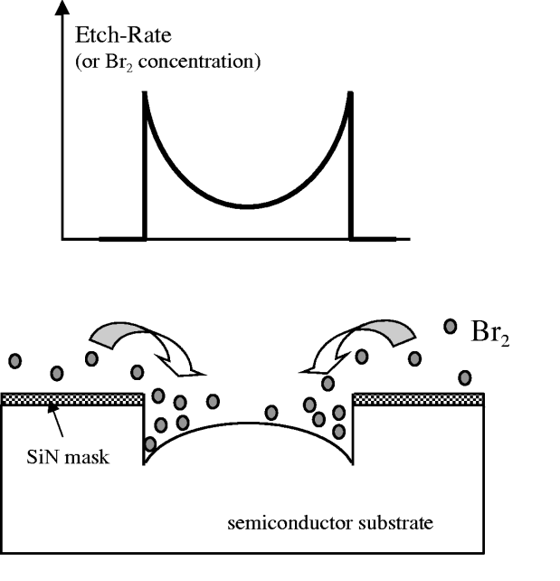
diffusion-limited etching. Fabrication of our circular microlenses began with the deposition of 1000-Å-thick plasma-enhanced chemical vapor deposition (PECVD) SiN film on a semiconductor substrate. Subsequently, circular holes with an appropriate diameter size were formed in the SiN film by standard photolithography and reactive-ion etching (RIE). The patterned sample was then immersed in a diffusion-limited etchant, which in our study was obtained by mixing HBr : H2O2 : H2O in the ratio of 2 : 1 : 60. After a desired etch time, the sample was removed from the etch-bath and thoroughly rinsed in deionized water. The SiN etch mask can be subsequently etched off in HF or by RIE if necessary. Fig. 1 schematically illustrates the etch process inside a mask hole. Br2 molecules do not react with the substrate in the masked region, and those molecules must diffuse into the open area—circular holes in our case—for etch. Due to the low mobility of Br2 molecules, however, the probability that the molecules are consumed is higher near the mask boundary than far away from it. Such gradual spatial variation in the etch rate across the etch window (whose distribution is schematically depicted in the upper panel of Fig. 1) forms a spherical lens profile on the semiconductor surface. During the etch period, which depends on the semiconductor material and the desired lens curvature, the sample needs to sit static inside the etch bath for good reproducibility since any disturbance against the natural diffusive motion of the etching species would alter the details of the etching process.

Fig1
For a detailed quantitative evaluation of lens profile, we employed the AFM technique. Fig. 3 shows the full-scale perspective image of the GaAs microlens, constructed from the measured AFM data. Represented in Fig. 4(a) is the lens profile along the line passing through the center of the lens, which is also reconstructed from the 2-D AFM data. The dotted line is a theoretical fit based on the spherical lens approximation. The radius of curvature of the lens and the focal length estimated from the fit are 91 and 36 m, respectively. A similar analysis for the InP microlens yields a radius of curvature of 159 m and a focal length of 69 μm.
上一篇: 通过在玻璃上旋涂的低温晶圆键合